

Method for preparing microcrystalline glass/glass carrier material having nano holes in high density
A technology of glass-ceramics and carrier materials, applied in the field of preparation of carrier materials, can solve problems such as low strength and poor size controllability, and achieve the effect of high strength, dense lattice, easy control and mastery
- Summary
- Abstract
- Description
- Claims
- Application Information
AI Technical Summary
Problems solved by technology
Method used
Image

Examples
example 1
[0018] Example 1: A method for preparing high-density nanoporous glass-ceramic / glass carrier material, comprising the following steps:
[0019] 1. Preparation of high-density nanoporous glass-ceramic substrate: take the glass-ceramic system as Li 2 O-SiO 2 -Al 2 o 3 -K 2 O-Na 2 O, its weight percentage is respectively 12.0, 78.5, 5.5, 3.0, 1.0; add additive, additive is TiO 2 , AgO, CeO 2 , SnO 2 , Sb 2 o 3 , AuCl, the percentages of each component in the total weight of glass-ceramics and additives are: 0.6, 0.15, 0.015, 0.005, 0.5, 0.0015; each required compound is weighed according to the proportion, and it is prepared after melting and molding at 1490°C Take a sample with a thickness of 0.9mm and a length and width of 25×50mm, and then shield and expose it under a UV lamp with a power of 500w for 15min. The distance between the glass substrate and the light source is 25cm. After heat treatment for 45min, the crystal phase is Li 2 SiO 3 The glass-ceramic, and th...
example 2
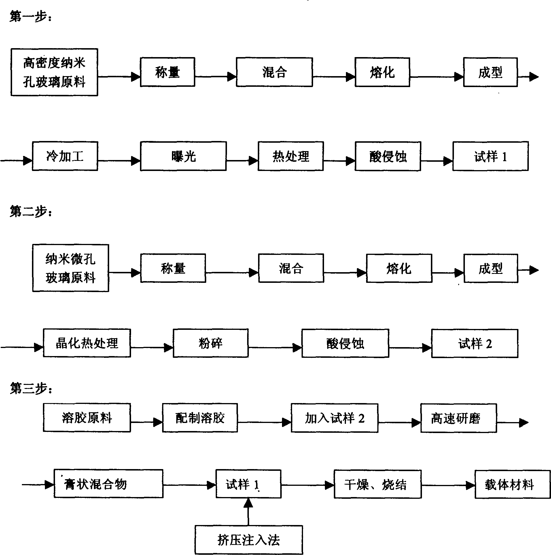
[0024] Example 2: if figure 1 Shown, a kind of method for preparing high-density nanoporous glass-ceramic / glass carrier material, comprises the following steps:
[0025] 1. Preparation of high-density nanoporous glass-ceramic substrate: a) Melting of glass: take the glass-ceramic system as Li 2 O-SiO 2 -Al 2 o 3 -K 2 O-Na 2 O, whose weight percent is 11.5Li respectively 2 O, 79.5SiO 2 , 5.3Al 2 o 3 , 2.5K 2 O, 1.2Na 2 O, plus additive, the additive is TiO 2 , AgO, CeO 2 , SnO 2 , Sb 2 o 3 , AuCl, the percentages of each component in the total weight of glass-ceramics and additives are: 0.5TiO 2 , 0.05AgO, 0.035CeO 2 , 0.005SnO 2 , 0.2Sb 2 o 3 , 0.001AuCl; weigh each required compound according to the proportion, melt and mold at 1450°C, and the thickness of the molded sample is 0.5mm; b) UV exposure: shield and expose the molded samples according to the required arrangement , the light source for UV exposure is an ultraviolet lamp, the power is 500w, the e...
example 3
[0028] Example 3: A method for preparing high-density nanoporous glass-ceramic / glass carrier material, comprising the following steps:
[0029] 1. Preparation of high-density nanoporous glass-ceramic substrate: a) Melting of glass: take the glass-ceramic system as Li 2 O-SiO 2 -Al 2 o 3 -K 2 O-Na 2 O, its weight percentage is respectively 12.5, 78.0, 4.5, 3.0, 2.0; add additive, additive is TiO 2 , AgO, CeO 2 , SnO 2 , Sb 2 o 3 , AuCl, the percentages of each component in the total weight of glass ceramics and additives are respectively: 1.0, 0.2, 0.02, 0.005, 0.5, 0.002; after weighing each required compound according to the proportion, melt and shape it at 1550 ° C, The thickness of the molded sample is 1.0mm; b) UV exposure: shield and expose the molded sample according to the required arrangement. The light source for UV exposure is an ultraviolet lamp with a power of 500w and an exposure time of 40min. The distance from the light source is 40cm; c) heat treatmen...
PUM
| Property | Measurement | Unit |
|---|---|---|
| thickness | aaaaa | aaaaa |
| pore size | aaaaa | aaaaa |
| thickness | aaaaa | aaaaa |
Abstract
Description
Claims
Application Information