Transmitter circuit, transmission circuit and driver unit

A technology for transmitting circuits and driving devices, which is applied in the connection/interface layout of logic circuits, transmission systems, digital transmission systems, etc., and can solve the problems of increased signal waveform distortion and inability to transmit signals.

Inactive Publication Date: 2005-02-02
RENESAS ELECTRONICS CORP
View PDF1 Cites 7 Cited by
  • Summary
  • Abstract
  • Description
  • Claims
  • Application Information

AI Technical Summary

Problems solved by technology

In addition, there is a problem that since the output capacitance of the transmission circuit and the input capacitance of the reception circuit are several pF, signal transmission can be performed even in a high-frequency region exceeding 100 MHz that does not yet belong to the high-definition or large-screen display panel. At the input end of the receiving circuit, the signal waveform distortion caused by the RC time constant will also increase, and good signal transmission cannot be performed

Method used


Image

  • Transmitter circuit, transmission circuit and driver unit
  • Transmitter circuit, transmission circuit and driver unit
  • Transmitter circuit, transmission circuit and driver unit

Examples


Embodiment Construction

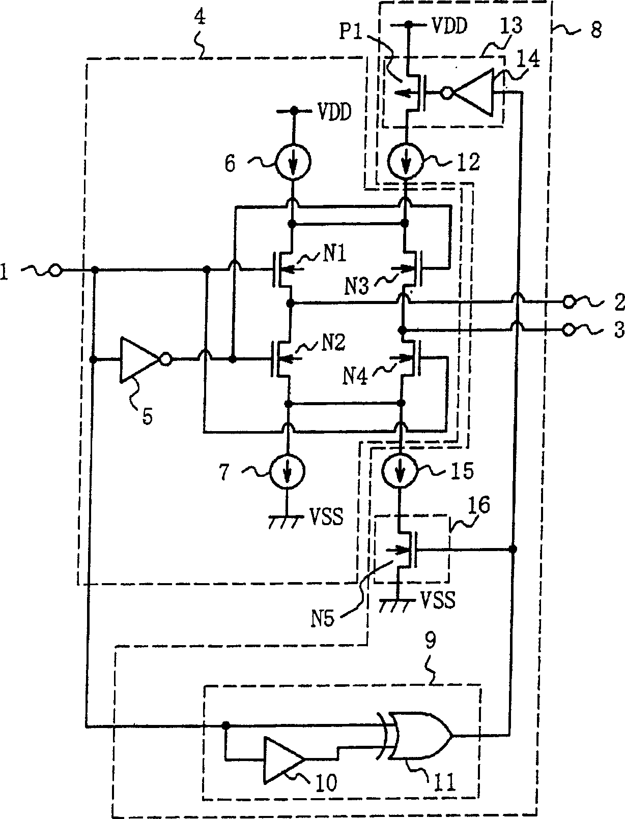
[0031] Next, embodiments of the present invention will be described with reference to the drawings. figure 1 It is a configuration diagram of the transmission circuit of the first embodiment of the present invention. Such as figure 1 As shown, the transmitting circuit of the first embodiment of the present invention has an input terminal 1, a non-inverting output terminal 2, an inverting output terminal 3, a driving circuit 4, and an output waveform control circuit 8.

[0032]The drive circuit 4 has a CMOS type inverter circuit 5, a constant current source 6 for source signal current, a constant current source 7 for sink signal current, N-channel MOS transistor N1, N-channel MOS transistor N2, N Channel type MOS transistor N3, N channel type MOS transistor N4. One end of the constant current source 6 is connected to the high potential side power supply VDD, and the other end of the constant current source 6 is connected to the drain terminal of the N-channel MOS transistor N1 an...


PUM


Abstract

Provided is a transmitter circuit capable of transmitting a signal at a high speed because signal waveform distortion in an input terminal of a receiving circuit is reduced even though a transmission path has a high resistance component such as aluminum wiring and cooper wiring on a glass substrate and to provide a transmission circuit and a driving device. The transmitter circuit comprises: a non-inverting output terminal and an inverting output terminal, for outputting a signal current, which has a loop direction that changes based upon an input signal, to the non-inverting and inverting output terminals; and an output-waveform control circuit for detecting the edge of the waveform of the input signal and responding by increasing the signal current temporarily.

Description

Technical field [0001] The present invention relates to a transmission circuit, a transmission circuit, and a driving device, and in particular, to a transmission circuit, a transmission circuit, and a driving device suitable for liquid crystal display devices, organic EL (electroluminescence) display devices, plasma display devices, and the like. Background technique [0002] In the past, in matrix type liquid crystal display devices, organic EL display devices, plasma display devices, etc., one horizontal line of gray scale data signal and scanning signal were sequentially generated from the inputted image signal of one frame, and then output timing control. The LSI (Large Scale Integrated Circuit) and the signal source driver LSI, which is a driving device that receives the grayscale data signal and drives each data line of the display panel, are mounted on the printed wiring board together. The timing controller LSI and the signal The signal transmission between the source dr...

Claims


Application Information

Patent Timeline
Patent Type & Authority Applications(China)
IPC IPC(8): G09G3/20H03F3/16H03K5/1534H03K17/687H03K19/0175H04L25/02
CPCG09G2310/0267H04L25/0286H03K5/1534G09G3/20G09G2310/0275H04L25/0272G09G2370/08
Inventor 细川朗央西村浩一
Owner RENESAS ELECTRONICS CORP
Why Eureka
Try Eureka