Substrate for optical element, organic electroluminescence element and organic electroluminescence display device
A technology of optical elements and light-transmitting substrates, which is applied in the field of organic electroluminescent display devices, and can solve the problems of increasing the area where an electric field cannot be applied, insufficient light extraction efficiency, and ineffective extraction.
- Summary
- Abstract
- Description
- Claims
- Application Information
AI Technical Summary
Problems solved by technology
Method used
Image
Examples
example 1
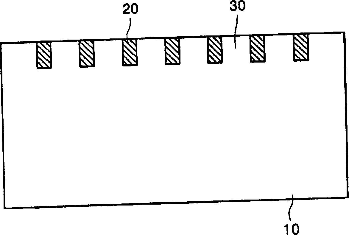
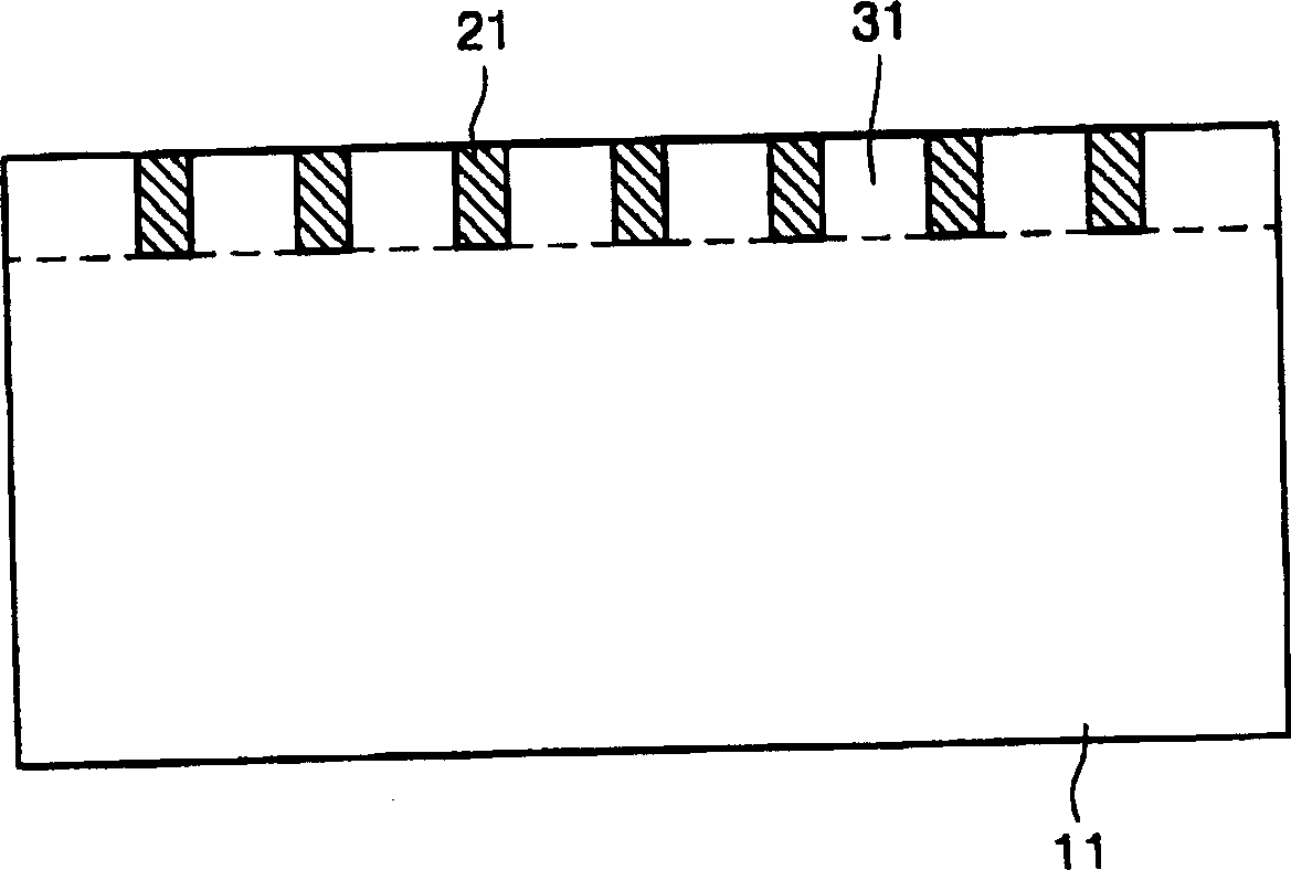
[0075] A positive type resist material was formed to a thickness of 4000 Å on a quartz substrate (refractive index: 1.457) using a spin coater as a photoresist material, and then patterned using a photomask.
[0076] As a light source, a Hg-Xe lamp (wavelength: 250 nm) was used. Here, a stripe mask pattern with a period of 1.0 μm, a line width of 0.75 μm, and a space width of 0.25 μm was used. Using this mask, after exposure once, the mask was rotated by 90° and exposed again under the same conditions. After this exposure, the mask is treated with an alkaline developer to form a resist pattern. As a result of SEM observation, it was confirmed that the target grating pattern could be produced. The quartz substrate attached to the fabricated resist pattern was etched by reactive gas etching (Samuco, RIE1ONR). Under the condition of 100W output, use CF 4 (4Pa, 20SCCM) for etching. Etching was performed to form a trench of 10000 Å on the quartz substrate during 2080 seconds. ...
example 2
[0083] A positive-type resist material with a thickness of 4000 Å was formed on a quartz substrate (refractive index: 1.457) using a spin coater as a photoresist material, and then the formed photoresist was detected by a two-flux laser interference exposure system. The resist is exposed. As a laser light source used in this two-flux laser interference exposure system, an Ar ion laser (wavelength: 488 nm) was used, and exposure was performed under the following conditions.
[0084] The laser light is divided into two luminous fluxes with a beam splitter, and the interference exposure is carried out using a reflector, so that the intersection angle on the substrate surface becomes about 31 degrees (laser luminous intensity: 100mA / cm 2 , exposure time: 15 seconds). After performing this exposure once, the substrate was rotated by 90°, and exposure was performed again using the same conditions.
[0085] After exposure, it was processed by an alkaline developer AZ300MIF (manufac...
PUM
 Abstract
Description
Claims
Application Information


