
Self-ionized and inductively-coupled plasma for sputtering and resputtering

A plasma and inductive coupling technology, used in sputtering plating, electro-solid devices, ion implantation plating, etc., can solve problems such as insufficient bottom coverage

Inactive Publication Date: 2005-05-25
APPLIED MATERIALS INC
View PDF15 Cites 6 Cited by
  • Summary
  • Abstract
  • Description
  • Claims
  • Application Information

AI Technical Summary

Problems solved by technology

Long range provides ample sidewall coverage, but bottom coverage may not be sufficient

Method used


Image

  • Self-ionized and inductively-coupled plasma for sputtering and resputtering
  • Self-ionized and inductively-coupled plasma for sputtering and resputtering
  • Self-ionized and inductively-coupled plasma for sputtering and resputtering

Examples


Embodiment Construction

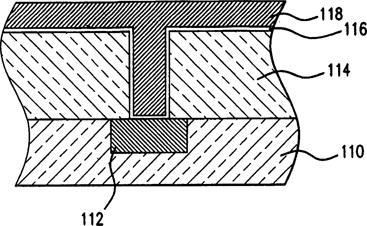
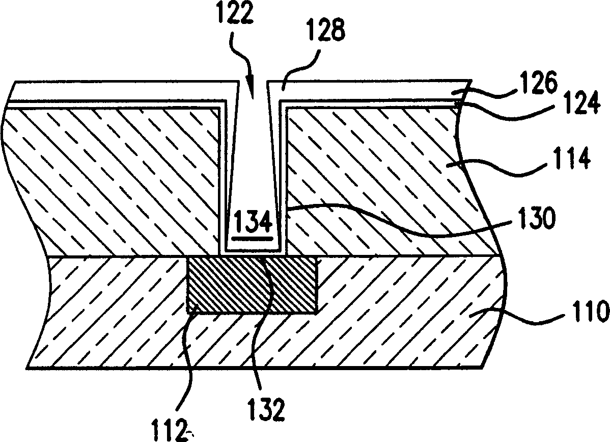
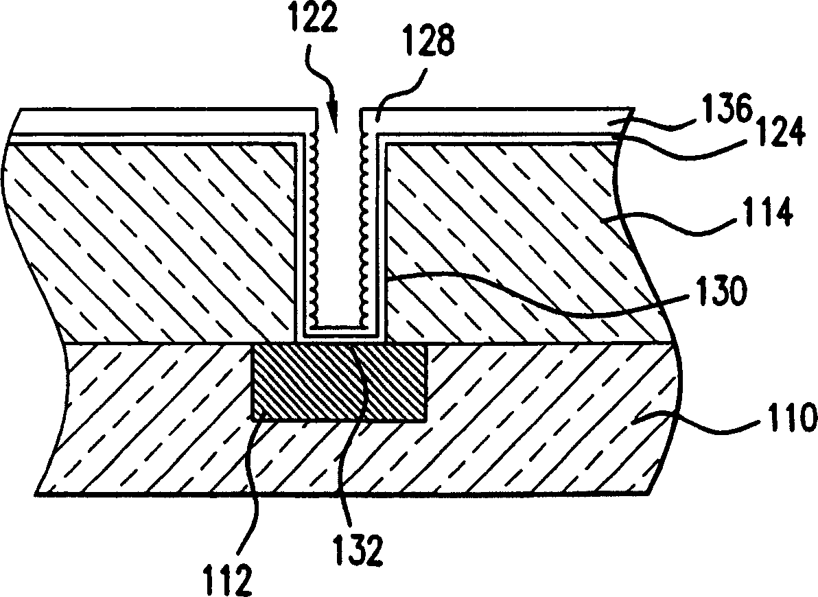
[0045] The distribution between sidewall and bottom cover in a DC magnetron sputtering reactor is suitable for making metal layers such as lining layers with desired profiles in holes or vias in dielectric layers. SIP films sputter-deposited into high-aspect-ratio vias can have good upper sidewall coverage and are less prone to protrusions. Bottom coverage can be thinned or eliminated by re-sputtering of the ICP at the bottom of the via, if desired. According to one version of the invention, the advantages of both types of sputtering can be obtained in a reactor which preferably combines a selected solution of SIP and ICP plasma generation techniques in the separation step. Examples of such reactors are Figure 4 150 summary instructions in . In addition, depositing the coil material onto the substrate by sputtering the ICP coil 151 located within the chamber keeps the upper portion of the liner layer sidewalls free from re-sputtering.

[0046] Reactor 150 may be used to dep...


PUM


Abstract

A magnetron sputtering reactor for sputter deposition of materials such as, for example, tantalum, tantalum nitride, and copper, wherein self-ionized plasma (SIP) sputtering and inductively coupled plasma ( ICP) sputtering, both together or either, are facilitated in the same chamber. In addition, bottom coverage can be thinned or eliminated by re-sputtering by ICP. SIP is facilitated by a small magnetron with non-uniform magnetic strength poles and high power applied to the target during sputtering. ICP is provided by one or more RF coils that inductively couple RF energy into the plasma. The combined SIP-ICP layer can act as a liner or barrier or seed or nucleation layer for the holes. Additionally, the RF coil can be sputtered to provide protective material during ICP re-sputtering.

Description

[0001] related application [0002] This application claims priority to Provisional Application Serial No. 60 / 342,608, filed December 21, 2001, and Provisional Application Serial No. 60 / 316,137, filed August 30, 2001, which are hereby incorporated by reference in their entirety. technical field [0003] The present invention generally relates to sputtering and re-sputtering. In particular, the present invention relates to sputter deposition of materials and re-sputtering of deposited materials in the formation of semiconductor integrated circuits. Background technique [0004] Semiconductor integrated circuits generally include multiple layers of metallization to provide electrical connections between a large number of active semiconductor devices. Advanced integrated circuits, especially those used in microprocessors, may include five or more layers of metallization. Previously, aluminum was a popular metallization, but copper has been developed as a metallization for adv...

Claims


Application Information

Patent Timeline
IPC IPC(8): C23C14/04C23C14/34C23C14/35H01J37/32H01J37/34H01L21/28H01L21/285H01L21/3205H01L21/768H01L23/52
CPCC23C14/046C23C14/345C23C14/3457C23C14/358H01J37/321H01J37/3408H01J2237/3327H01L21/2855H01L21/76805H01L21/76844H01L21/76846H01L21/76862H01L21/76864H01L21/76865H01L21/76868H01L21/76873H01L21/76877H01L2221/1089H01J37/32C25D5/02C23C14/34C23C14/35
Inventor P·丁Z·徐R·C·莫塞利S·伦加拉詹N·迈蒂D·A·卡尔B·秦P·F·史密斯D·安杰洛A·托利亚J·傅F·陈P·戈帕拉贾X·唐J·C·福斯特
Owner APPLIED MATERIALS INC
Learn More