
Field emitting electronic source device and its preparing process

An electron source and field emission technology, which is used in the manufacture of electrical components, discharge tube electron guns, electrode systems, etc., can solve the problems of emission current divergence, difficulty in obtaining high-quality insulating layers, and difficulty in wide application.

Inactive Publication Date: 2005-08-10
OCEAN UNIV OF CHINA
View PDF0 Cites 4 Cited by
  • Summary
  • Abstract
  • Description
  • Claims
  • Application Information

AI Technical Summary

Problems solved by technology

where the MIM structure is as Figure 4 As shown, it has the advantages of low driving voltage (less than 20V), small divergence angle of emission current, and low requirement for vacuum degree, etc., but has low emission current density and low efficiency (the control gate current is much higher than the emission current) These shortcomings are mainly due to the difficulty in obtaining high-quality insulating layers, resulting in high leakage currents at the gate; the electron source of the MOS structure is similar to the MIM structure, only using semiconductor silicon materials to obtain high-quality SiO2 insulating layers, but the actual results Indicates that the problems with the MIM structure have not been resolved
The electron source of the metal microtip structure with the microtip cathode as the electron emission region is shown in Figure 5. It has the advantages of high emission current density, relatively low driving voltage (less than 100V), high efficiency, etc., and is a newly developed structure in recent years. It is also the focus of current research, but there are problems such as high driving voltage (about 70V), serious emission current divergence (divergence angle greater than 30 degrees), and complicated process, making it difficult to achieve wide application.

Method used


Image

  • Field emitting electronic source device and its preparing process
  • Field emitting electronic source device and its preparing process
  • Field emitting electronic source device and its preparing process

Examples


Embodiment Construction

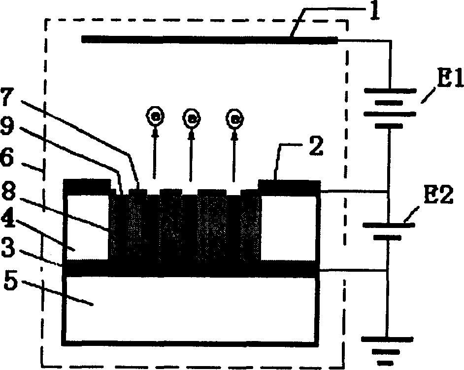
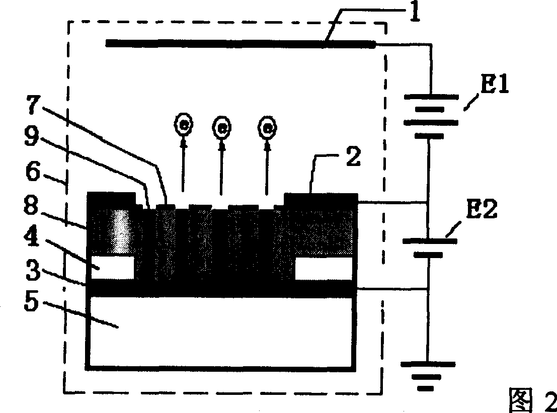
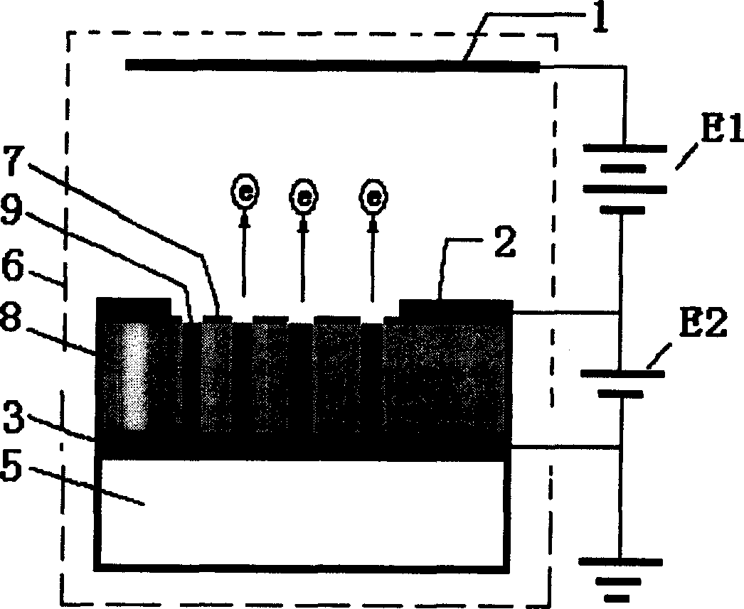
[0016] The present invention has an anode 1 sealed in a vacuum container 6 and a field emission electron source comprising a cathode 3 on a substrate 5 and a grid 2 and its interlayer structure. It is characterized in that the thick metal film (referred to as thick Metal film) and the cathode 3 is an insulating layer 4, and between the thin metal film 7 with a large number of micropores connected to the thick metal film and the cathode 3 is a complex layer 8, that is, the field emission electron source is the cathode 3 There is an insulating layer 4 on it, and a part of the insulating layer 4 is replaced by a complex layer 8, and a network-shaped thin metal film 7 with a large number of micropores is used as a part of the gate 2 on the composite layer 8. Such as figure 1 As shown, the thin metal film 7 is a metal film with a thickness within 50 nanometers and a large number of micropores with a pore diameter within 1 micron as the electrode of the gate 2, so as to technically...


PUM

PropertyMeasurementUnit
Thicknessaaaaaaaaaa
Apertureaaaaaaaaaa

Abstract

The disclosed device consists of electron source of field emission and anode sealed in vacuum container. The electron source includes cathode, grid pole and interlayer prepared on base plate. Insulation layer is positioned between thick metallic membrane, which leads out grid pole, and cathode. Compound body layer is located between thin metallic membrane of possessing large numbers of micropores connected to the said thick metallic membrane and cathode. Interlayer structure includes insulation layer, semiconductor layer and compound body layer positioned between cathode and grid layer. Preparation method includes steps: preparing compound body layer on the cathode fabricated on base plate of silicon or glass etc. through microelectronic technique; preparing grid pole of thin metallic membrane on compound body layer; sealing the prepared device and anode in vacuum container. Advantages are simple technique, reasonable structure, low driving current and high emissivity etc.

Description

technical field [0001] The invention relates to a field emission electron source device and a preparation method thereof. Background technique [0002] Currently, field emission electron sources used and researched mainly include metal microtips (Spindt microtips), metal-insulator-metal (MIM) and metal-insulator-semiconductor (MOS) structures. where the MIM structure is as Figure 4 As shown, it has the advantages of low driving voltage (less than 20V), small divergence angle of emission current, and low requirement for vacuum degree, etc., but has low emission current density and low efficiency (the control gate current is much higher than the emission current) These shortcomings are mainly due to the difficulty in obtaining high-quality insulating layers, resulting in high leakage currents at the gate; the electron source of the MOS structure is similar to the MIM structure, only using semiconductor silicon materials to obtain high-quality SiO2 insulating layers, but the a...

Claims


Application Information

Patent Timeline
IPC IPC(8): H01J1/304H01J3/02H01J9/02H01J37/06
Inventor 元光宋航
Owner OCEAN UNIV OF CHINA
Learn More