Dielectric layer for semiconductor device and method of manufacturing the same

A dielectric layer and semiconductor technology, applied in semiconductor/solid-state device manufacturing, semiconductor devices, electric solid-state devices, etc., can solve problems related to dielectric materials, reduce channel mobility, and reduce device performance

Active Publication Date: 2005-08-17
SAMSUNG ELECTRONICS CO LTD
View PDF4 Cites 261 Cited by
  • Summary
  • Abstract
  • Description
  • Claims
  • Application Information

AI Technical Summary

Problems solved by technology

[0007] However, these attempts have not solved the problems associated with conventional dielectric materials
For example, a silicon nitride layer or a silicon oxynitride layer between a high-k dielectric layer and a silicon substrate or a polysilicon gate causes high interface state density charge trapping, thereby reducing channel mobility and degrading device performance

Method used


Image

  • Dielectric layer for semiconductor device and method of manufacturing the same
  • Dielectric layer for semiconductor device and method of manufacturing the same
  • Dielectric layer for semiconductor device and method of manufacturing the same

Examples


Embodiment Construction

[0017] The present invention provides a stable (noble) dielectric layer structure and a manufacturing method thereof. In the following description, many specific details are explained to provide a comprehensive understanding of the present invention. However, those of ordinary skill in the art should understand that the present invention can still be implemented without using these details. In some examples, well-known process steps, device structures and technologies are not shown in detail to avoid making the present invention difficult to understand.

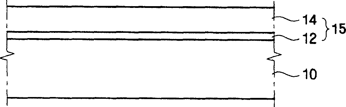
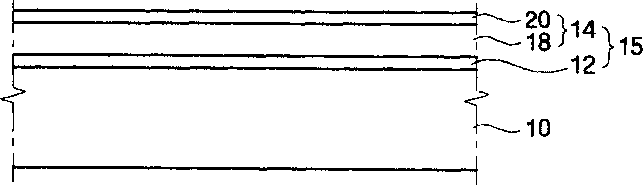
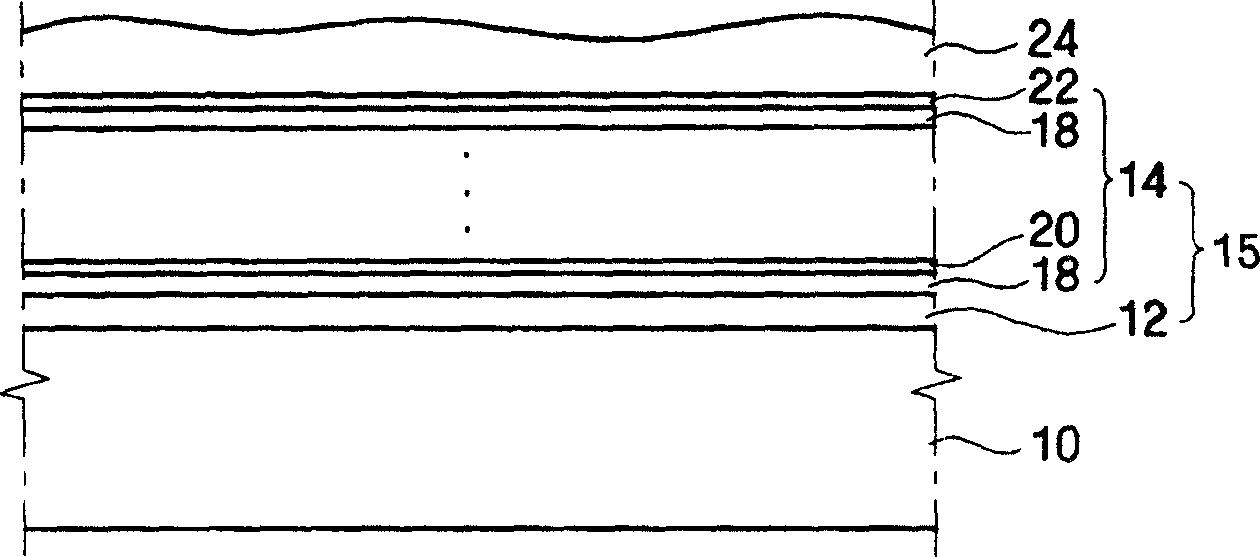
[0018] reference figure 1 According to an embodiment of the present invention, the silicate interface layer 12 formed of silicate material may be disposed on the conductive layer or the semiconductor substrate 10, such as a silicon substrate. The dielectric constant of the silicate interface layer 12 is preferably greater than any one of silicon oxide, silicon nitride, or silicon oxynitride. Preferably, the silicate interface la...


PUM

PropertyMeasurementUnit
thicknessaaaaaaaaaa
thicknessaaaaaaaaaa
thicknessaaaaaaaaaa

Abstract

A semiconductor device comprises a silicate interface layer and a high-k dielectric layer overlying the silicate interface layer. The high-k dielectric layer comprises metal alloy oxides.

Description

Technical field [0001] Generally speaking, the present invention relates to the field of semiconductor devices, and more specifically, to a multilayer dielectric structure, a semiconductor device using the multilayer dielectric structure, and a manufacturing method thereof. Background technique [0002] With each occurrence of metal oxide semiconductor (MOS) integrated circuits (ICs), the size of devices continues to decrease to provide high-density and high-performance devices. In particular, since the driving current in a MOS field effect transistor (FET) increases as the thickness of the gate dielectric decreases, the thickness of the gate dielectric becomes as small as possible. Thus, in order to improve device performance, it has become increasingly important to provide extremely thin, reliable, and low-defect gate dielectrics. [0003] For decades, thermal oxide layers, such as silicon dioxide (SiO 2 ), has been used as the gate dielectric, because the silicon dioxide therm...

Claims


Application Information

Patent Timeline
Patent Type & Authority Applications(China)
IPC IPC(8): C23C16/42H01L21/28H01L21/316H01L21/336H01L21/822H01L21/8242H01L21/8247H01L27/04H01L27/108H01L27/115H01L29/51H01L29/78H01L29/786H01L29/788H01L29/792
Inventor 李钟镐李来寅
Owner SAMSUNG ELECTRONICS CO LTD
Why Eureka
Try Eureka