

Integral probe card and assembling mode
A probe card and probe technology, applied in the field of probe cards, can solve problems such as affecting test stability, small probe deformation ability, and easy signal error.
- Summary
- Abstract
- Description
- Claims
- Application Information
AI Technical Summary
Problems solved by technology
Method used
Image

Examples
Embodiment Construction
[0041] see Figure 1 to Figure 1 1. An integrated probe card (100), which provides a preferred embodiment of the present invention, mainly includes a plurality of predetermined number of probes (10), a circuit space converter (20), and a flexible circuit communication connection board (30), a circuit board (40) and a level adjustment mechanism (50), wherein:
[0042] These probes (10) are made by following steps:
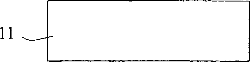
[0043] Step 1. Prepare the base material: figure 1 As shown, take a sheet-like wafer substrate (11) (note: it is a side section shown in the figure), and complete necessary pre-treatments such as cleaning and drying (the substrate used in this embodiment ( 11) is a silicon wafer).
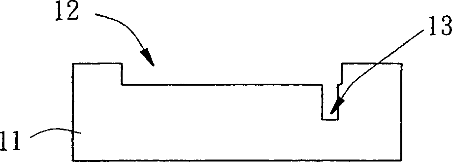
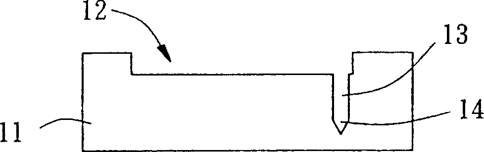
[0044] Step 2. Etching recesses on the substrate: if figure 2 As shown, the geometric shape and position of the probe tip (Probe tip) are precisely defined by using the lithography process (Lithography Process; LIGA), and then the anisotropic etching (anisotropicetching) is carried ...
PUM
 Abstract
Description
Claims
Application Information