Sample-analyzing device and process for manufacturing the same

A technology for inspection devices and samples, which is applied in the direction of measuring devices, chemical instruments and methods, biochemical equipment and methods, etc., can solve the problems of large reaction field, low detection accuracy, inability to form hybrids efficiently, and achieve the realization of Miniaturization and analysis of the effect of cost reduction

Inactive Publication Date: 2005-10-19
PANASONIC CORP
View PDF4 Cites 3 Cited by
  • Summary
  • Abstract
  • Description
  • Claims
  • Application Information

AI Technical Summary

Problems solved by technology

In this way, the reaction field is extremely large relative to the size of the gene to be analyzed and the immobilized DNA, so a large amount of sample solution is required for one reaction tank
In addition, if the sample is insufficient, the hybrid cannot be formed efficiently, and the detection accuracy may decrease
[0022] In addition, the above-mentioned problems exist not only in the technical field related to the analysis using the DNA chip, but also when trying to refine and increase the density of the reaction field on the sample mounting surface at the above-mentioned high level, exist

Method used


Image

  • Sample-analyzing device and process for manufacturing the same
  • Sample-analyzing device and process for manufacturing the same
  • Sample-analyzing device and process for manufacturing the same

Examples


no. 1 approach

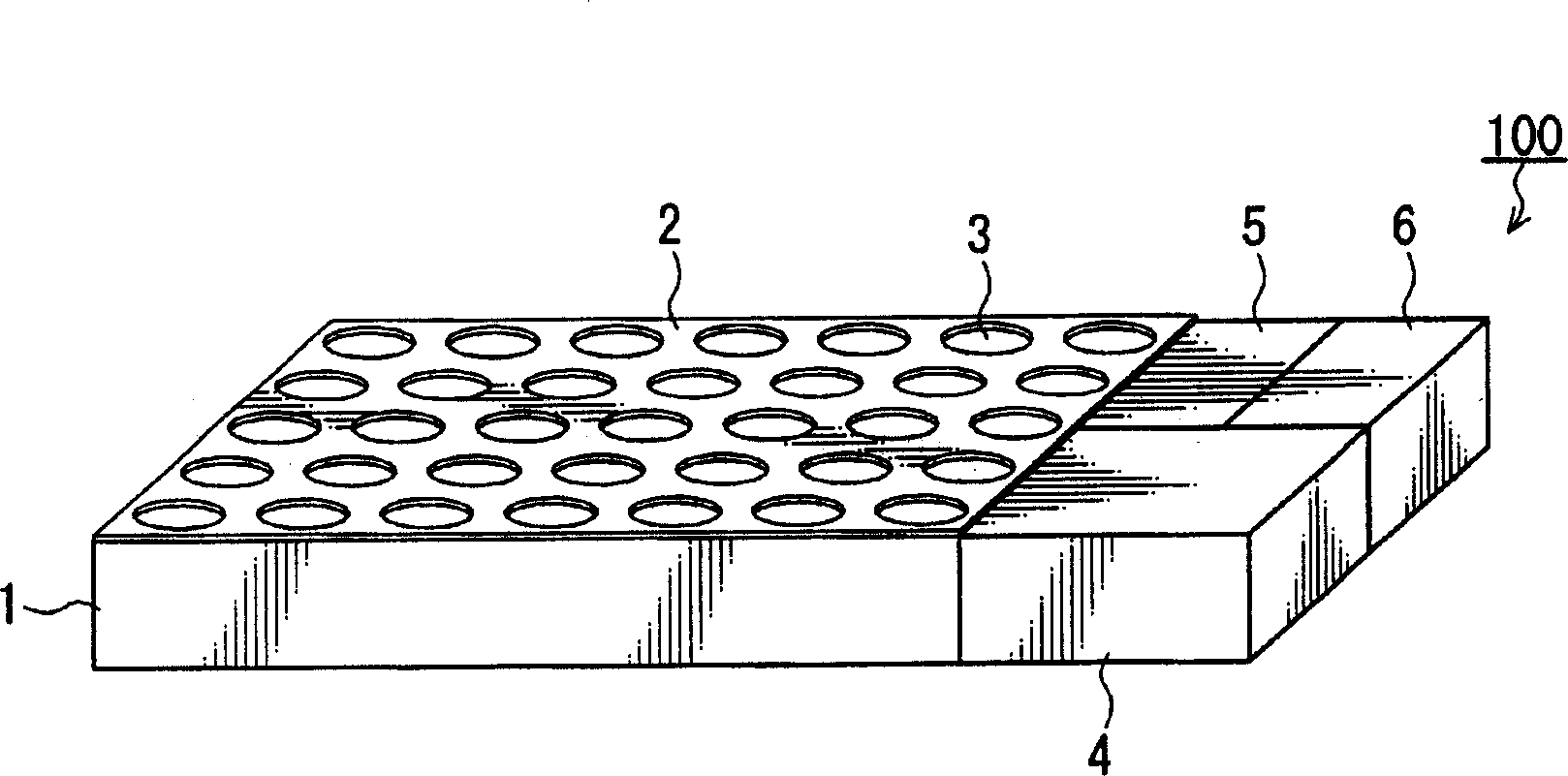
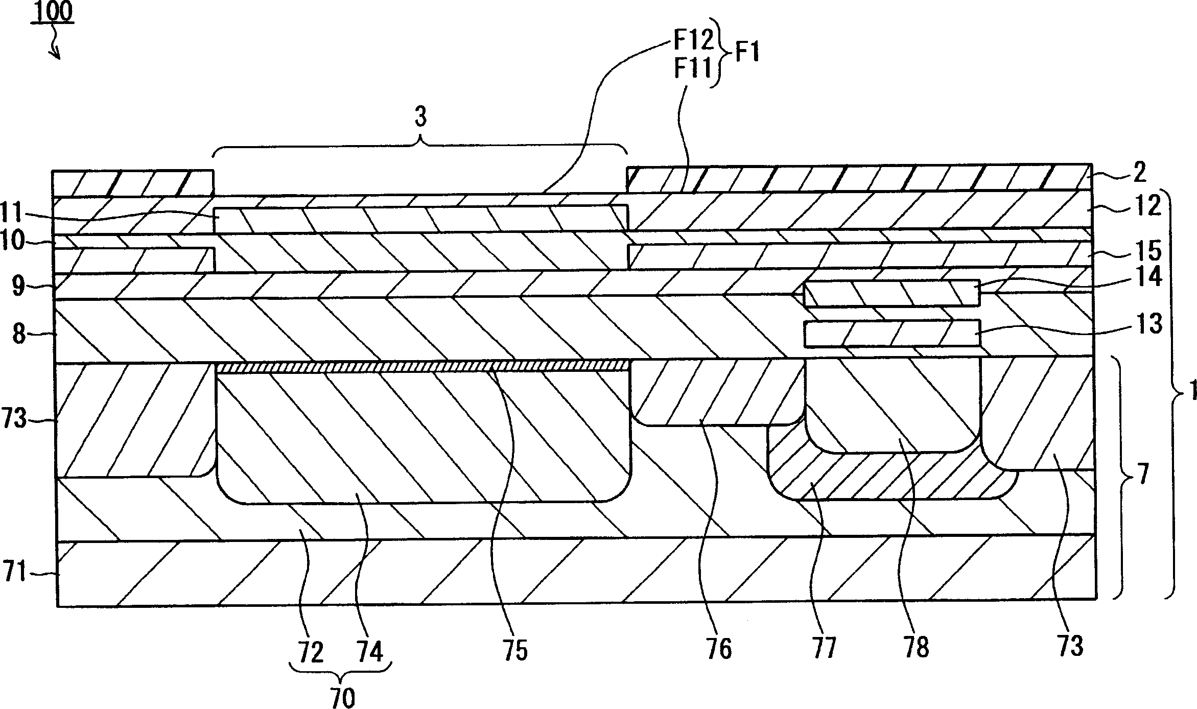
[0110] figure 1 It is a perspective view showing the first embodiment of the sample inspection device of the present invention. figure 2 to express roughly figure 1 A partial cross-sectional view of the basic configuration of the sample inspection device shown. Such as figure 1 and figure 2 As shown, the sample inspection device 100 includes a plate-shaped substrate 1 (semiconductor integrated circuit substrate). The plate-shaped substrate 1 has a sample mounting surface F1. A plurality of recesses 3 of a plurality of liquid droplets of the object to be measured are analyzed. In addition, the sample inspection device 100 further includes a CPU 4 , a storage unit 5 , and a data input / output unit 6 integrally provided on the side surface of the substrate 1 .

[0111] Such as figure 2 As shown, the sample mounting surface F1 is divided into at least a first region F11 covered with a hydrophobic monomolecular film 2 and a plurality of hydrophilic second regions F12 not co...

no. 2 approach

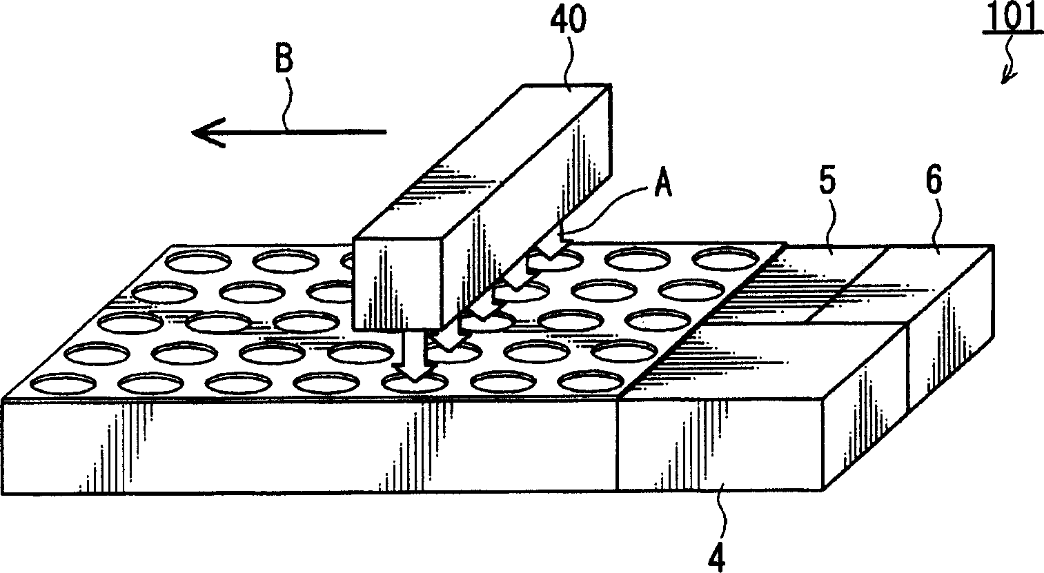
[0274] A second embodiment of the sample inspection device of the present invention will be described below. The sample inspection device 101 of this second embodiment has the following structure, such as figure 1 and figure 2 As shown, in the sample inspection device 100 of the first embodiment, there is also a droplet supply unit 40 (ink jet head) for ejecting a droplet containing an object to be analyzed and measured facing the concave portion 3. of the nozzle. The configuration other than the droplet supply unit 40 is the same as that of the sample inspection device 100 of the first embodiment. The CPU 4 serves as a control unit that adjusts the position of the nozzle relative to the recess 3 by moving the nozzle of the droplet supply unit 40 . That is, the droplet supply unit 40 has a drive mechanism that arbitrarily changes its relative position with respect to the sample mounting surface F1 under the control of the CPU 4 .

[0275] The droplet supply unit 40 will b...

Embodiment 1

[0328] Below, according to use Figure 8 ~ Figure 10 To illustrate the sequence, make a with Figure 7 The sample inspection device 102 shown is a sample inspection device having the same configuration.

[0329] Prepared by semiconductor thin film manufacturing technology with figure 2 Substrate 81 (semiconductor integrated circuit substrate, main surface size: 15 mm × 25 mm, thickness: 0.8 mm) with the same configuration as substrate 1 shown, the number of photodiodes arranged two-dimensionally at equal intervals: 120,000, arranged two-dimensionally at equal intervals Density of photodiodes: 37000 / cm2 ).

[0330] Then, according to the monomolecular film forming step according to the present invention, the monomolecular film 83 was formed on the main surface (the surface serving as the sample mounting surface) of the substrate 81 in the following procedure.

[0331] First, the main surface of the substrate 81 is washed with ultrapure water, and droplets of ultrapure water...


PUM

PropertyMeasurementUnit
volumeaaaaaaaaaa
thicknessaaaaaaaaaa
volumeaaaaaaaaaa

Abstract

This sample inspection device 100 is provided with at least one substrate 1 having a sample mounting face F1 provided with two or more of recesses 3 for storing independently two or more of liquid drops containing a measuring object to be analyzed. The face F1 is partitioned at least into the first area F11 coated with a hydrophobic monomolecular film 2, and the second areas F12 having an inside not coated with the monomolecular film 2 and having a hydrophilic property. A bottom face of the each of the recesses 3 is formed of the F12, and the whole outer circumferential portion including the whole inner face of the each recess 3 is formed of the monomolecular film 2 coating the F11. The film 2 is formed of an organic molecule, and is immobilized onto the face F1 with a covalent bond.

Description

technical field [0001] The present invention relates to a sample inspection device for performing analysis by detecting a luminescence reaction generated in a droplet containing an object to be analyzed and measured such as a specific gene or a specific protein, and a method for manufacturing the same. Background technique [0002] In recent years, DNA chips and DNA microarrays (hereinafter referred to as "DNA chips") have been widely used as new means of gene analysis for the purpose of diagnosis and prevention of diseases, drug development, and the like. As a DNA chip, it is generally as follows: on a glass substrate, droplets of a DNA solution containing a DNA probe of a known gene sequence are printed on a surface of a droplet for immobilizing a sample (hereinafter referred to as "" On the sample loading surface"), a DNA chip in which various DNA probes are immobilized at high density; a DNA chip in which DNA probes are immobilized by synthesizing DNA on a glass substrat...

Claims


Application Information

Patent Timeline
Patent Type & Authority Applications(China)
IPC IPC(8): B01L3/00G01N21/25
CPCB01J2219/00722B01J2219/00585B01J2219/00725B01J2219/0036B01J2219/00621G01N21/253B01L3/5088C40B60/14B01J2219/00626B01J19/0046B01J2219/00283C40B40/10B01J2219/00619B01J2219/00497B01J2219/00364B01J2219/00317B82Y30/00B01J2219/00527B01J2219/00596B01J2219/00711C03C17/38B01J2219/00576C40B40/06B01J2219/00605B01J2219/00677B01J2219/00734B01L2200/12B01L3/5085B01J2219/00441B01J2219/00432B01J2219/00385B01J2219/00743B01J2219/00378B01J2219/00382B01J2219/00659
Inventor 美浓规央
Owner PANASONIC CORP
Why Eureka
Try Eureka