United measuring system and its measuring technology for scanning channel microscope and scanning micro electrode

A scanning tunneling and measurement system technology, applied in the field of scanning tunneling microscope and scanning microelectrode combined measurement, can solve the problems of lack of sensitivity to chemical properties of surface microregions, difficulty in interpretation of SPM images, interrelated physical and chemical properties, etc.

Inactive Publication Date: 2005-10-19
XIAMEN UNIV
View PDF0 Cites 12 Cited by
  • Summary
  • Abstract
  • Description
  • Claims
  • Application Information

AI Technical Summary

Problems solved by technology

[0003] However, with the deepening of research and the development of science and technology, several key drawbacks and deficiencies of scanning microprobe (SPM) technology have become more and more apparent. A single scanning microprobe technology has been difficult to meet complex comprehensive research. Due to the observation of highly oriented surface structures, it is difficult to interpret the SPM images of most polycrystalline or amorphous materials; SPM is only sensitive to the surface microscopic appearance, but lacks the sensitivity of the chemical properties of the surface micro-regions, and the surface microscopic appearance is difficult to detect. Correlates with physicochemical properties of surface domains

Method used


Image

  • United measuring system and its measuring technology for scanning channel microscope and scanning micro electrode
  • United measuring system and its measuring technology for scanning channel microscope and scanning micro electrode
  • United measuring system and its measuring technology for scanning channel microscope and scanning micro electrode

Examples


Embodiment Construction

[0014] The present invention will be described in detail below through examples.

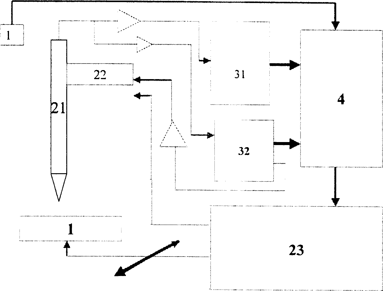
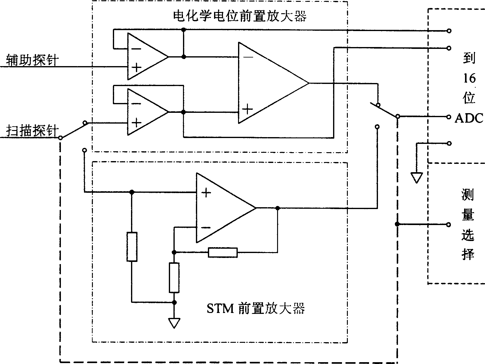
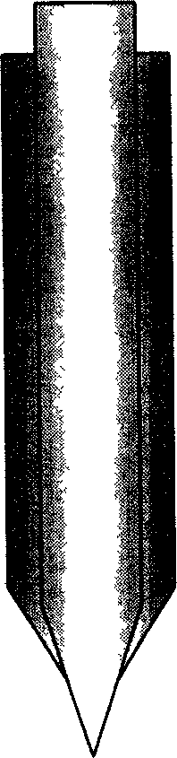
[0015] The scanning tunneling microscope and scanning microelectrode combined measurement system consists of 4 units: scanning tunneling microscope (STM) measurement platform, scanning microprobe and control / drive unit: tunneling current signal and micro-area potential signal measurement unit and measurement signal Control and processing unit. The STM measurement platform is an open commercial STM instrument, see figure 1 , the scanning micro-probe and the control / driving unit include a scanning micro-probe 21, an X-Y-Z three-dimensional piezoelectric micro-scanner 22 and a stepping motor-driven X-Y two-dimensional mechanical scanner 23, wherein the scanning micro-probe is a Pt with a diameter of 0.3mm -Ir alloy wire (see image 3 ), using the mechanical shearing method to prepare the tip of the scanning microprobe, the diameter of which is in the order of nanometers, and encapsulating the tip...


PUM

PropertyMeasurementUnit
diameteraaaaaaaaaa

Abstract

The present invention relates to measurement system and measurement technology with combined scanning tunnel microscope (STM) and scanning micro electrode. The measurement system consists of STM measuring platform, scanning micro probe and control/driving unit; tunnel current signal and micro area potential signal measuring unit; and measuring signal controlling and processing unit. The present invention utilizes micro scanning probe in simultaneous detection of surface tunnel current and surface potential distribution, adopts scanning mode interchange between micro piezoelectric scanning and mechanical step motor scanning, and uses tunnel current as indication of micro scanning electrode reaching the surface of sample, to realize the quantitative control of the distance between the tip of micro scanning electrode and the sample surface and to raise the spatial resolution in the measurement. The present invention provides opened platform for various surface spatial resolution measuring technology.

Description

technical field [0001] The invention relates to a combined measurement technology of a scanning tunnel microscope and a scanning micro-electrode. Background technique [0002] In 1982, International Business Machines Corporation (IBM) Zurich Laboratory Binnig and others successfully developed the first Scanning Tunneling Microscope (STM), the basic principle of which is to use the tunneling effect in quantum theory to detect samples by scanning microprobes The surface electron density distribution can be obtained indirectly to obtain the surface morphology of the sample. The emergence of STM makes it possible to obtain the surface topography and structure with atomic spatial resolution in situ and in real time. STM has further stimulated the continuous introduction of various other scanning microprobe microscopy (SPM) technologies, and has greatly The earth has promoted the rapid development of the entire nanotechnology. So far, SPM has become one of the most powerful tool...

Claims


Application Information

Patent Timeline
Patent Type & Authority Applications(China)
IPC IPC(8): G01Q60/14
Inventor 林昌健李彦卓向东胡融刚
Owner XIAMEN UNIV
Why Eureka
Try Eureka