Optic micro distance correcting method

A correction method and macro-distance technology, applied in optics, optomechanical equipment, and originals for optomechanical processing, etc., can solve problems such as unprovided, difficult operation, and reduced optical process margins

Active Publication Date: 2005-10-19
TAIWAN SEMICON MFG CO LTD
View PDF0 Cites 2 Cited by
  • Summary
  • Abstract
  • Description
  • Claims
  • Application Information

AI Technical Summary

Problems solved by technology

Figure 1A A partial mask pattern showing 4 lines a, b, a', b' including 4 line ends, where lines a and b are a pair of adjacent lines that lie on another pair of adjacent lines a' and b ', and lines a, b are a small distance from lines a' and b'; in this case, OPC does not provide these four line ends so as not to modify the line ends of this mask pattern ; Usually the reason why OPC is not added is that after adding OPC structure between lines, the margin of optical process will be reduced, resulting in operational difficulties

Method used


Image

  • Optic micro distance correcting method
  • Optic micro distance correcting method
  • Optic micro distance correcting method

Examples


Embodiment Construction

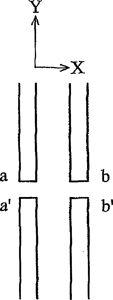
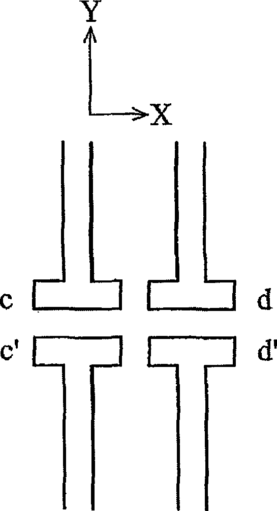
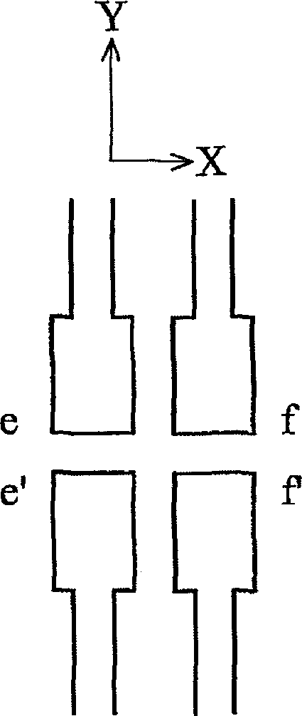
[0036] This disclosure describes an improved OPC technique for correcting end-of-line distortion / offset due to optical macro effects in semiconductor manufacturing. This disclosed method uses an asymmetric structure as the serif of OPC to improve the general method, and the serif has no or little damage to the margin of the optical photolithography and line etching process, so as to avoid the connection between the line end and the line end. shortened problem.

[0037] Figure 2A to Figure 2D Describe how this disclosure uses an asymmetric OPC structure for OPC processing. The size and shape of the OPC structure disclosed in the present disclosure do not have to be symmetrical to effectively correct the line distortion / offset, but some better orientations and asymmetrical OPC structures are used to correct the line distortion / offset.

[0038] Figure 2A It is an example of an asymmetrical OPC structure. Part of the mask pattern includes 4-line ends. The 4-line ends are a pa...


PUM


Abstract

The invention discloses a method for conducting optical proximity correction, comprising the steps as follow: one end of a first element pattern is detected, wherein, the end is near to one end of a second element pattern, and then a first optical proximity correction pattern which is toward to a first direction is added onto the first element pattern; and a second optical proximity correction pattern which is toward to a second direction is added onto the second element pattern, wherein, the second direction is basically reverse to the first direction. The invention relates to an improved OPC technique so as to correct the line-end distortion or departure due to the optical proximity effect during the semiconductor production. As a non-symmetric structure is used as the lining line of the OPC technique, the invention has no harm or only small harm on the optical photolithography and the line-etching allowance, thereby avoiding the problems such as line-end connection or line-end shortening.

Description

technical field [0001] The present disclosure relates to the fabrication of a semiconductor device, and more particularly to a method for correcting line-width and line-space offsets in a photolithography process for aligning circuit components with The pattern is transferred onto the substrate of the semiconductor element. Background technique [0002] The manufacture of semiconductor integrated circuits (IC) and components requires many photolithography process steps to define and produce specific circuit components and circuit layouts on the substrate layer. Common photolithography systems will The specific circuit and / or composition image on the mask pattern reticle is projected onto the flat base material layer coated with a photosensitive film (photoresist), after the image is exposed, and then The film is developed to transfer circuits and / or components onto the base layer, and the patterned substrate is then processed by various techniques such as etching and doping...

Claims


Application Information

Patent Timeline
Patent Type & Authority Applications(China)
IPC IPC(8): G03C5/00G03F1/14G03F7/00G03F9/00H01L21/027H01L21/66
CPCG03F1/36G03F1/144
Inventor 廖忠志
Owner TAIWAN SEMICON MFG CO LTD
Why Eureka
Try Eureka