Substrate processing apparatus

一种基板处理装置、基板的技术,应用在气态化学镀覆、加热元件材料、涂层等方向,能够解决膜厚增加等问题,达到防止污染、提高生产率、防止裂纹的效果

Inactive Publication Date: 2005-10-19
TOKYO ELECTRON LTD
View PDF1 Cites 1 Cited by
  • Summary
  • Abstract
  • Description
  • Claims
  • Application Information

AI Technical Summary

Problems solved by technology

The problem of increasing the film thickness accompanying the heat treatment of the base oxide film 12 becomes a very serious problem especially when the film thickness of the base oxide film 12 is preferably reduced to a few atomic layers or less as the base oxide film.

Method used


Image

  • Substrate processing apparatus
  • Substrate processing apparatus
  • Substrate processing apparatus

Examples


Embodiment Construction

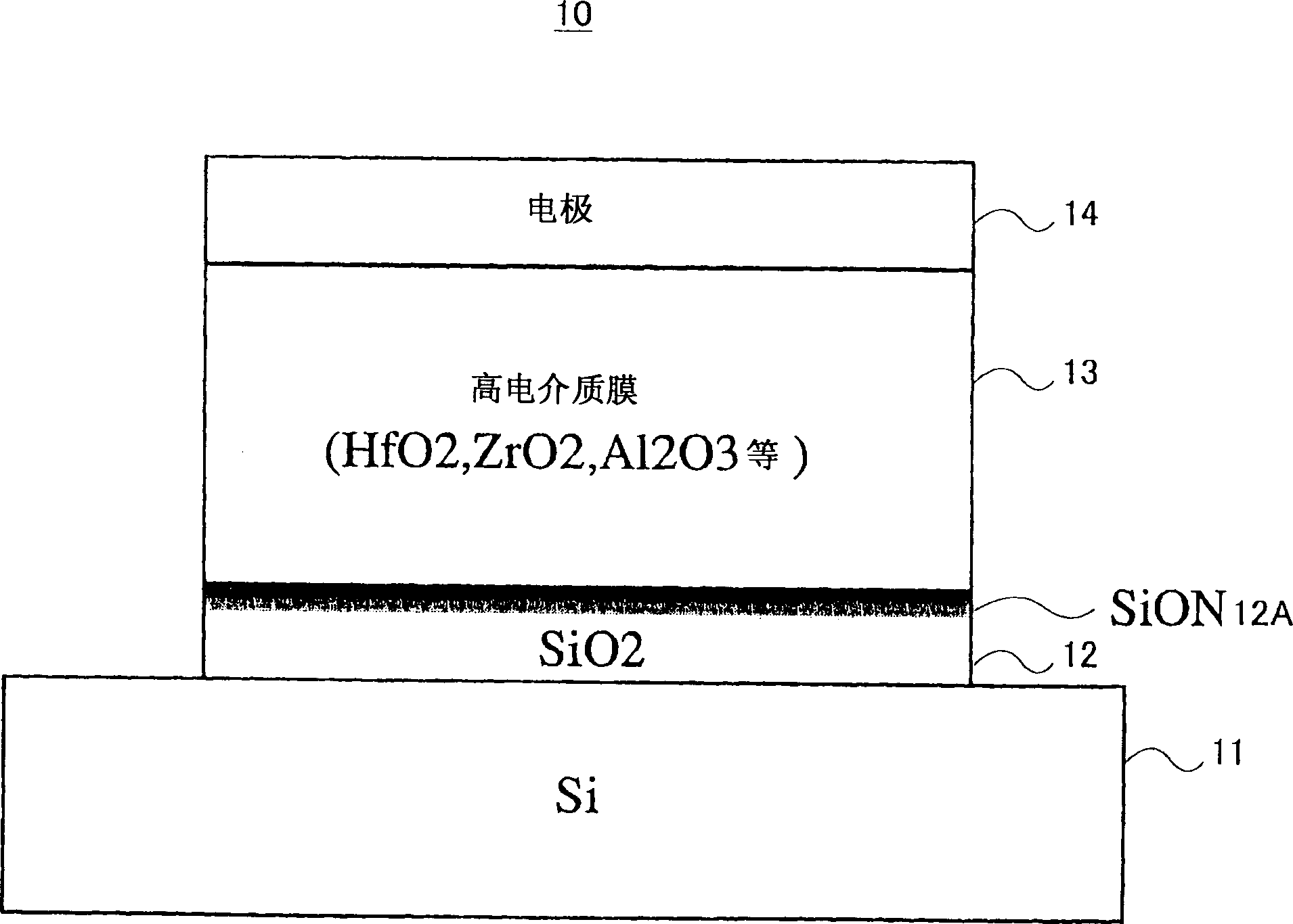
[0114] with the following Figure 1 Embodiments of the present invention will be described first.

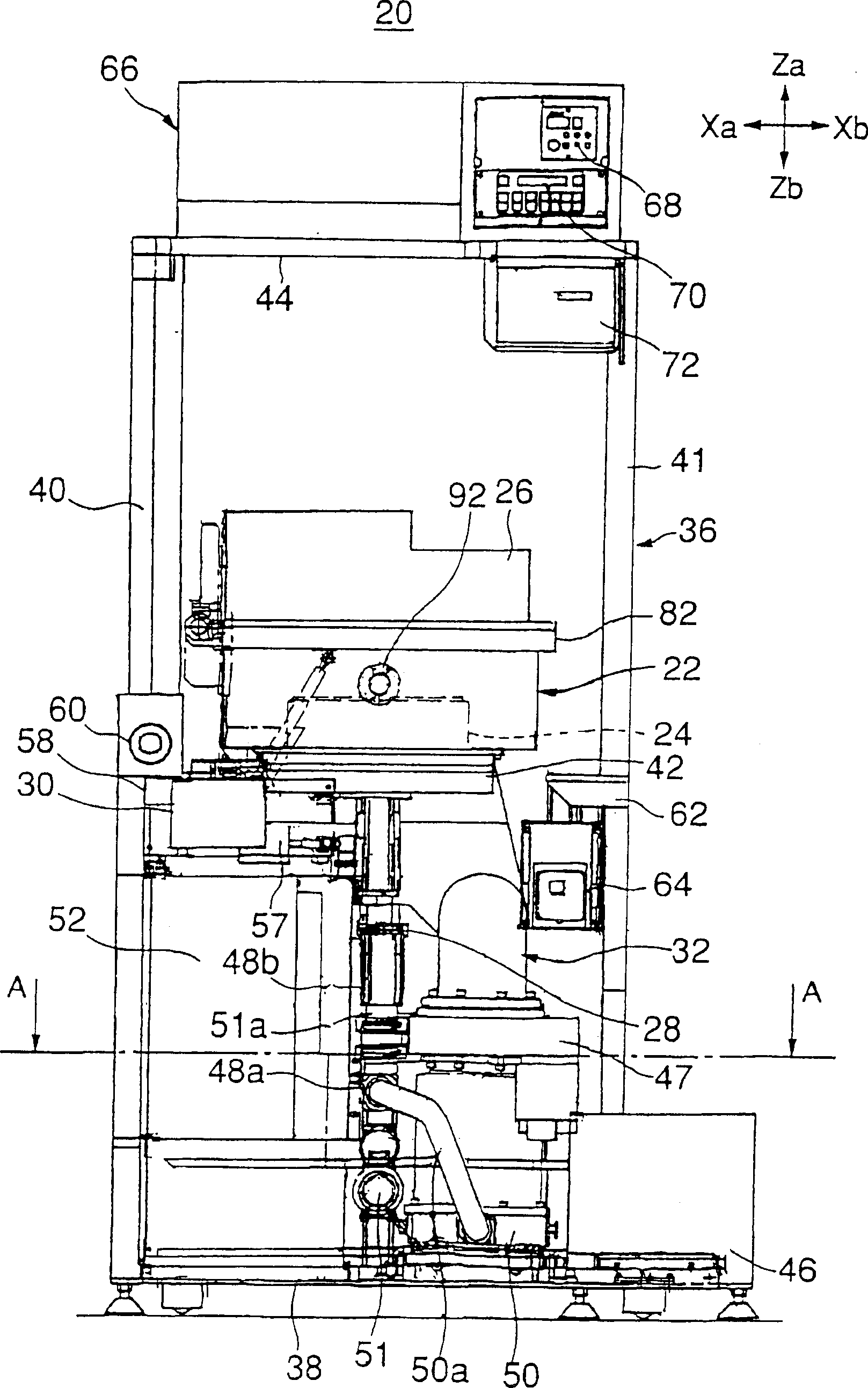
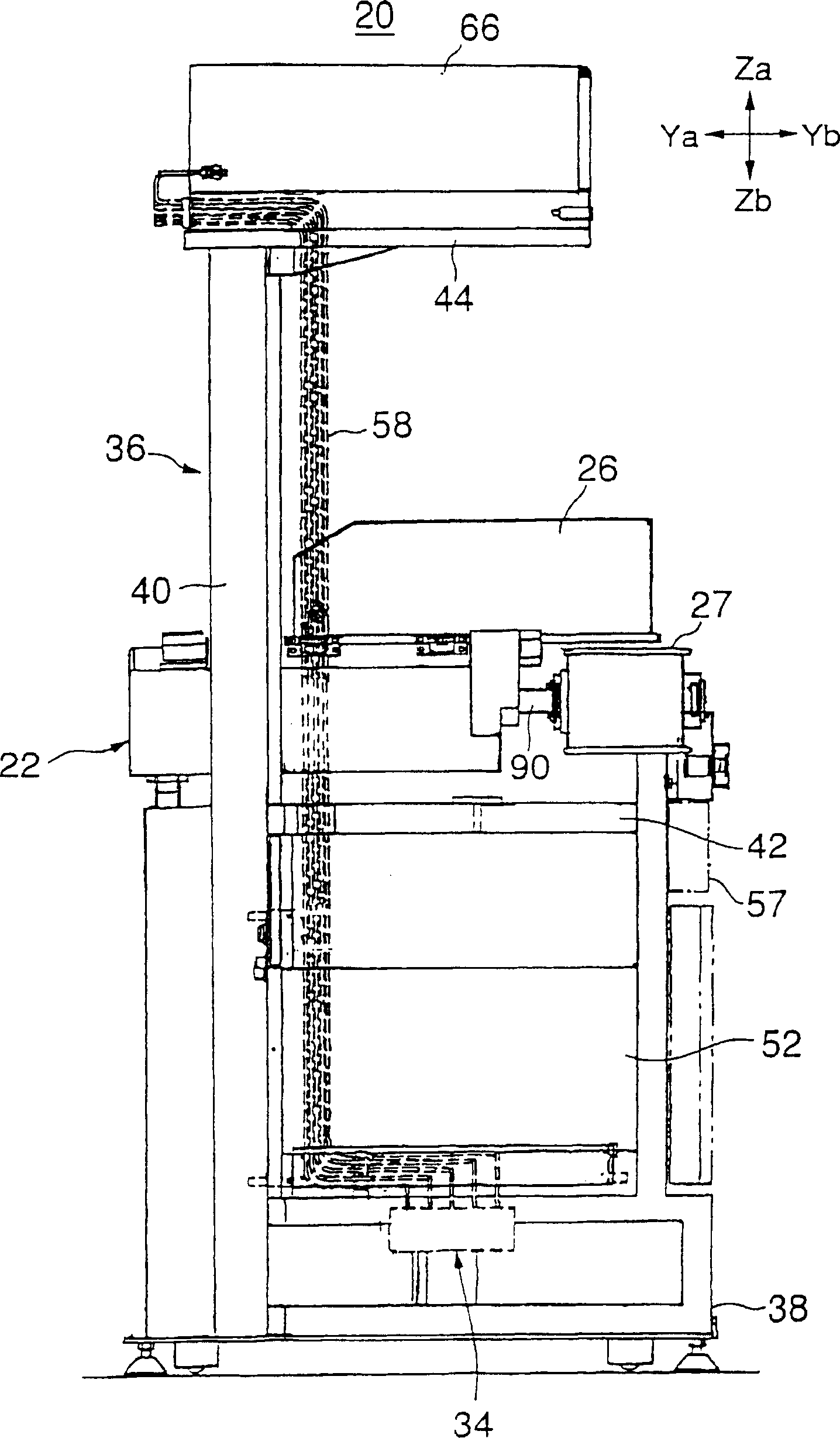
[0115] figure 2 It is a front view showing the structure of an embodiment of the substrate processing apparatus of the present invention. image 3 It is a side view showing the structure of one embodiment of the substrate processing apparatus of the present invention. Figure 4 for along figure 2 A cross-sectional view of line A-A in the center.

[0116] Such as Figure 2 to Figure 4As shown, the substrate processing apparatus 20 can continuously carry out the ultraviolet light radical oxidation treatment of the silicon substrate and the free radical oxidation film formed by such ultraviolet light radical oxidation treatment using a high-frequency remote plasma as described later. The method of base nitriding treatment constitutes.

[0117] The main structure of the substrate processing apparatus 20 includes a processing container 22 forming a processing space inside, a ...


PUM

PropertyMeasurementUnit
wavelengthaaaaaaaaaa
coating thicknessaaaaaaaaaa

Abstract

The substrate processing apparatus according to the present invention is aimed to stably and efficiently perform a deposition process on a substrate W. The substrate processing apparatus supports the substrate W in a position facing a heater portion and thus rotates a holding member holding the substrate W. Furthermore, the heating portion houses a SiC heater and a heat reflecting member in an internal portion of a quartz bell jar made of transparent quartz, and depressurizes an internal space of a processing vessel and an internal space of the quartz bell jar at the same time; thereby allowing the thickness of the quartz bell jar to be thinner, and thus improving thermal conductivity of heat from the SiC heater and preventing contamination by the SiC heater.

Description

technical field [0001] The present invention relates to a substrate processing apparatus, in particular to a substrate processing apparatus for performing processes such as film formation on a substrate. Background technique [0002] Today, in ultra-high-speed semiconductor processing devices, it is possible to develop a gate length of less than 0.1 μm along with the development of miniaturization processes. In general, the operating speed of semiconductor devices increases with miniaturization. However, in such miniaturized semiconductor devices, the thickness of the gate insulating film needs to be reduced according to the law of proportionality due to the shortening of the gate length due to miniaturization. [0003] However, if the gate length is less than 0.1 μm, the thickness of the gate insulating film must be set at 1 to 2 nm or less when using the existing thermal oxide film, but with such a very thin gate insulating film, the tunnel The current increases, and as a...

Claims


Application Information

Patent Timeline
Patent Type & Authority Applications(China)
IPC IPC(8): H05B3/14C23C16/46C23C16/48H01L21/00H01L21/31H01L21/316
CPCH01L21/67103C23C16/481C23C16/4586H01L21/68785H01L21/67109
Inventor 堀口贵弘桑嶋亮
Owner TOKYO ELECTRON LTD
Why Eureka
Try Eureka