Semiconductor device capable of being connected to external terminals by wire bonding in stacked assembly

An external terminal, semiconductor technology, applied in the direction of semiconductor devices, semiconductor/solid-state device manufacturing, semiconductor/solid-state device components, etc., can solve the problems of increased signal propagation delay, increased transistor junction capacitance, and large transistor size, etc. Avoid the effect of increasing the area and increasing the speed

Inactive Publication Date: 2005-11-09
ELPIDA MEMORY INC
View PDF1 Cites 5 Cited by
  • Summary
  • Abstract
  • Description
  • Claims
  • Application Information

AI Technical Summary

Problems solved by technology

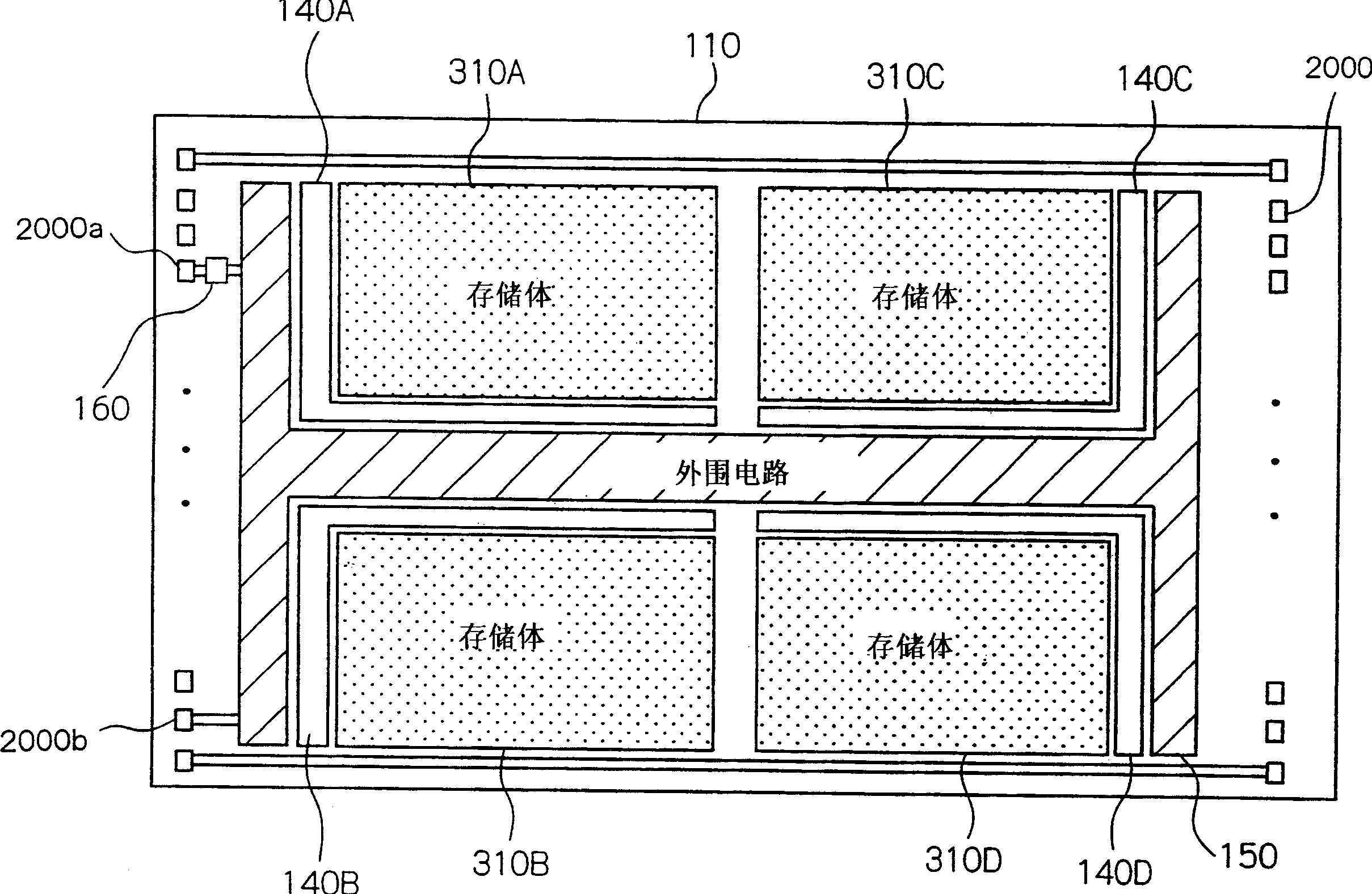
Also, since the output buffers are separated from each pad and connected there by wide interconnects, the capacitance of the interconnects is large
The size of the transistor serving as the output buffer of the final output stage circuit is large because the transistor needs to send a high-power signal to a wide interconnection, resulting in an increase in the junction capacitance of the transistor
Therefore, the propagation delay of the signal caused by the interconnected CR value increases

Method used


Image

  • Semiconductor device capable of being connected to external terminals by wire bonding in stacked assembly
  • Semiconductor device capable of being connected to external terminals by wire bonding in stacked assembly
  • Semiconductor device capable of being connected to external terminals by wire bonding in stacked assembly

Examples


no. 1 example

[0082] Figure 8A is a plan view showing the arrangement of the MCP according to the first embodiment of the present invention, and Figure 8B is Figure 8A An enlarged top view of the pad of the MCP shown in .

[0083] Such as Figure 8A As shown in , the MCP includes a lower memory chip 10 , an upper memory chip 20 and a CPU chip 30 as a component for controlling the lower and upper memory chips 10 , 20 . The lower and upper memory chips 10, 20 are of the same type and the same size. The lower memory chip 10 has pads 11a to 11e disposed close to and along one side 18 thereof. Similarly, the upper memory chip 20 has pads 21a to 21e disposed close to and along one side 28 thereof, and the CPU chip 30 has pads 31a to 31e disposed close to and along one side thereof.

[0084] The upper memory chip 20 is stacked on the lower memory chip 10 with the side 28 shifted in position from the side 18 in a direction perpendicular thereto so that the pads 11a to 11e of the lower memory c...

no. 2 example

[0134] According to a second embodiment of the present invention, one MCP includes three stacked memory chips.

[0135] Figure 15 An MCP according to a second embodiment of the invention is shown in cross-section.

[0136] Such as Figure 15 As shown in , the MCP has two flash memories 91, 92 and DRAM 90. DRAM 90 may be replaced by SRAM (Static Random Access Memory).

[0137] Such as Figure 15 As shown in , two memories 91, 92 are stacked one on top of the other, as in the case of the memory chip according to the first embodiment, and a DRAM 90 is stacked on a flash memory 91. As in the first embodiment, the flash memories 91, 92 and DRAM 90 are connected by wire bonding to perform desired operations between the flash memories 91, 92 and DRAM 90 . The pads of the flash memories 91, 92 connected to the pads of the DRAM 90 are associated therein in the same manner as heretofore, and the above connection will not be described in detail below.

[0138] As in the first embo...


PUM


Abstract

A semiconductor device includes a rectangular chip having four sides, wires connected respectively to different external terminals, and a bonding pad disposed along one of the four sides of the rectangular chip and directly connected to the wires for connection to the different external terminals. Since the different external terminals are bonded directly to the bonding pad by the wires, a signal input from one of the external terminals via one of the wires can be sent to the other external terminal via the other wire.

Description

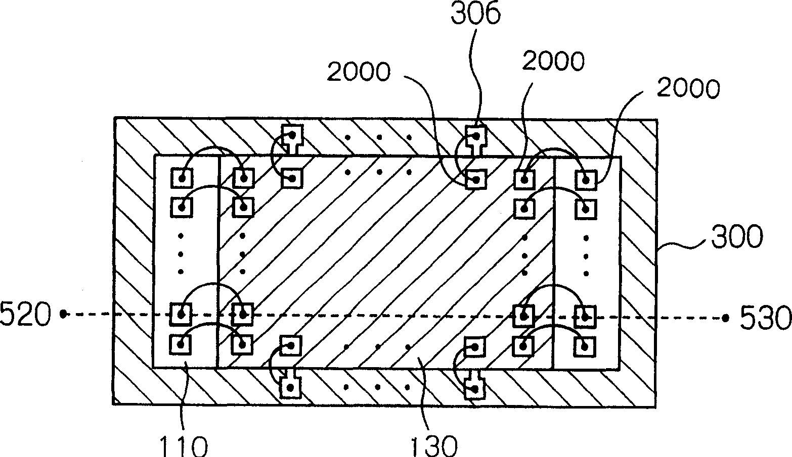
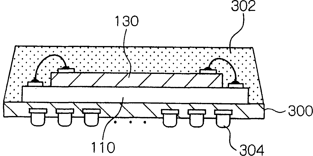
technical field [0001] The present invention relates to a semiconductor device, a multi-chip package including a stack of semiconductor devices, and a wire bonding method for interconnecting pads of the semiconductor devices. Background technique [0002] An example of a memory device called a stacked MCP (Multi-Chip Package) or MCP for short is disclosed in Japanese Laid-Open Patent Publication No. 2003-7963 (hereinafter referred to as Patent Document 1). Includes a stack of semiconductor devices such as RAM (random access memory) or flash memory. [0003] A conventional MCP will be described below, which includes a stack consisting of a memory chip in the form of a DRAM (Dynamic Random Access Memory) and a CPU (Central Processing Unit) as a component controlling the memory chip. [0004] 1A of the accompanying drawings is a plan view showing the internal structure of the MCP, and FIG. 1B is a cross-sectional view taken along the dotted line 520-530 of FIG. 1A. [0005] A...

Claims


Application Information

Patent Timeline
Patent Type & Authority Applications(China)
IPC IPC(8): H01L25/18H01L21/60H01L23/02H01L25/065H01L25/07
CPCH01L2924/01015H01L2224/4911H01L2924/01055H01L2924/15153H01L2924/01082H01L2924/00014H01L2225/06586H01L2924/01004H01L2924/01002H01L2924/30105H01L24/06H01L2924/15311H01L2225/06555H01L2224/48091H01L2224/05556H01L2224/48464H01L24/49H01L2924/01024H01L2224/48225H01L2924/19043H01L2924/3011H01L2224/85399H01L2224/48145H01L24/05H01L25/0657H01L2224/45099H01L2224/48227H01L2225/06527H01L2924/01005H01L2924/01033H01L2924/01006H01L2225/0651H01L2924/15165H01L2224/05599H01L2225/06562H01L2225/06506H01L24/48H01L2224/023H01L2224/04042H01L2224/05553H01L2224/05554H01L2224/85205H01L2924/181H01L2924/00H01L2924/00012H01L2924/0001
Inventor 中山晶智
Owner ELPIDA MEMORY INC
Why Eureka
Try Eureka