

Method of forming shallow trench isolation structure in a semiconductor device
A semiconductor and device technology, applied in the field of shallow trench isolation structure manufacturing, can solve problems such as connection leakage and device failure
- Summary
- Abstract
- Description
- Claims
- Application Information
AI Technical Summary
Problems solved by technology
Method used
Image

Examples
Embodiment Construction
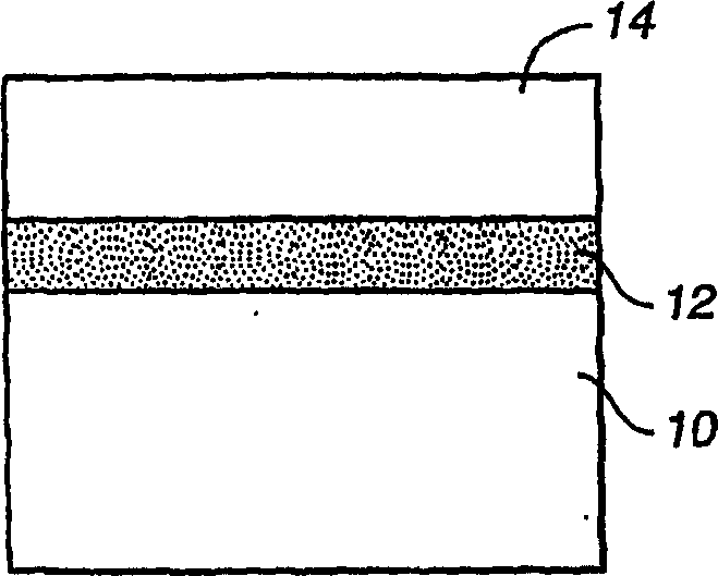
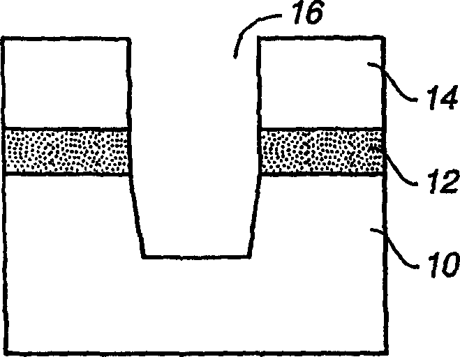
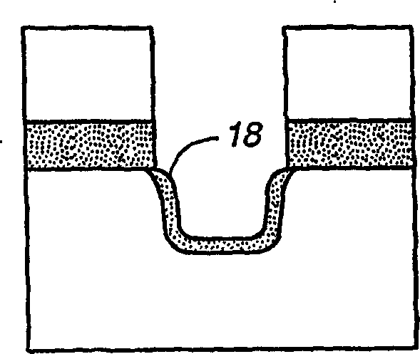
[0013] see Figure 3A According to the method for forming the shallow trench isolation structure of the present invention, the thermal oxidation of the surface of the silicon substrate 60 can form a thin layer of pad oxide 62 on the upper part of the silicon substrate 60 . A first nitride layer 64 is deposited on top of the pad oxide layer 62 to a thickness typically in the range of 100 Å to 500 Å, and the thickness of the pad oxide layer 62 is typically in the range of 50 Å to 200 Å, followed by a second layer of silicon oxide Layer 66 is deposited, typically at a thickness in the range of 100 Å-300 Å, and a second silicon nitride layer 68, typically at a thickness in the range of 1000 Å-2000 Å. In a typical process, silicon nitride layers 64 and 68 and oxide layer 66 are formed by low pressure chemical vapor deposition (LPCVD). like Figure 3B As shown, trench regions are first formed from a mask (not shown) formed on top of the second silicon nitride layer 68, and then sh...
PUM
 Abstract
Description
Claims
Application Information