High-temp. superconducting film conductor and preparing method thereof
A high-temperature superconducting and film-coating technology, applied in superconducting/high-conducting conductors, usage of superconducting elements, cable/conductor manufacturing, etc., can solve problems such as no successful reports and increased costs
- Summary
- Abstract
- Description
- Claims
- Application Information
AI Technical Summary
Problems solved by technology
Method used
Image

Examples
Embodiment 1
[0044] Sequential preparation of CeO on IBAD YSZ / Hast. substrates by an all-chemical solution method 2 Buffer layer and YBCO superconducting layer film. The final quench protection layer is prepared by magnetron sputtering technology.
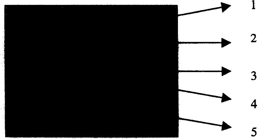
[0045] figure 1 : Schematic diagram of the cross-sectional structure of a high-temperature superconducting film-coated conductor. Among them: 1. Superconducting protective layer; 2. YBCO superconducting layer; 3. CeO 2 Buffer layer; 4. IBAD YSZ buffer layer; 5. Hastelloy metal substrate.
[0046] The superconducting protective layer is prepared by the conventional magnetron sputtering method; the YBCO superconducting layer is prepared by the TFA-MOD process, and the specific process is as follows:
[0047] 1) Prepare a YSZ buffer layer (commercially available) on a Hastelloy substrate using an IBAD process;
[0048] 2) Prepare CeO on the substrate described in 1) 2 The buffer layer;
[0049] CeO 2 The buffer layer is prepared by chemica...
Embodiment 2
[0066] Sequential preparation of CeO on IBAD YSZ / Hast. substrates by an all-chemical solution method 2 Buffer layer and YBCO superconducting layer film. The final quench protection layer is prepared by magnetron sputtering technology.
[0067] figure 1 : Schematic diagram of the cross-sectional structure of the high-temperature superconducting film-coated conductor.
[0068] Among them: 1. Superconducting protective layer; 2. YBCO superconducting layer; 3. CeO 2 Buffer layer; 4. IBAD YSZ buffer layer; 5. Hastelloy metal substrate.
[0069] The superconducting protective layer is prepared by the conventional magnetron sputtering method; the YBCO superconducting layer is prepared by the TFA-MOD process, and the specific process is as follows:
[0070] 1) Prepare a YSZ buffer layer (commercially available) on a Hastelloy substrate using an IBAD process;
[0071] 2) Prepare CeO on the substrate described in 1) 2 The buffer layer;
[0072] CeO 2 The buffer layer is prepared...
PUM
| Property | Measurement | Unit |
|---|---|---|
| Average roughness | aaaaa | aaaaa |
| Critical current density | aaaaa | aaaaa |
| Critical current density | aaaaa | aaaaa |
Abstract
Description
Claims
Application Information
 - R&D
- Intellectual Property
- Life Sciences
- Materials
- Tech Scout
- Unparalleled Data Quality
- Higher Quality Content
- 60% Fewer Hallucinations
Browse by: Latest US Patents, China's latest patents, Technical Efficacy Thesaurus, Application Domain, Technology Topic, Popular Technical Reports.
© 2025 PatSnap. All rights reserved.Legal|Privacy policy|Modern Slavery Act Transparency Statement|Sitemap|About US| Contact US: help@patsnap.com