Normal open type solid-state relay in high-speed switch

A solid state relay, high-speed switch technology, applied in electronic switches, electrical components, pulse technology and other directions, can solve the problem of no ATT1800 products, and achieve the effect of small output loss and simple input control circuit

Inactive Publication Date: 2006-02-01
BEIJING KEYTONE ELECTRONICS RELAY
View PDF3 Cites 19 Cited by
  • Summary
  • Abstract
  • Description
  • Claims
  • Application Information

AI Technical Summary

Problems solved by technology

The combination of ATT1800 and the introduced capacitor boosting technology can realize high-speed switching on and off of this type of solid state relay. After investigation, no ATT1800 product has been put into the market.

Method used


Image

  • Normal open type solid-state relay in high-speed switch
  • Normal open type solid-state relay in high-speed switch
  • Normal open type solid-state relay in high-speed switch

Examples


Embodiment Construction

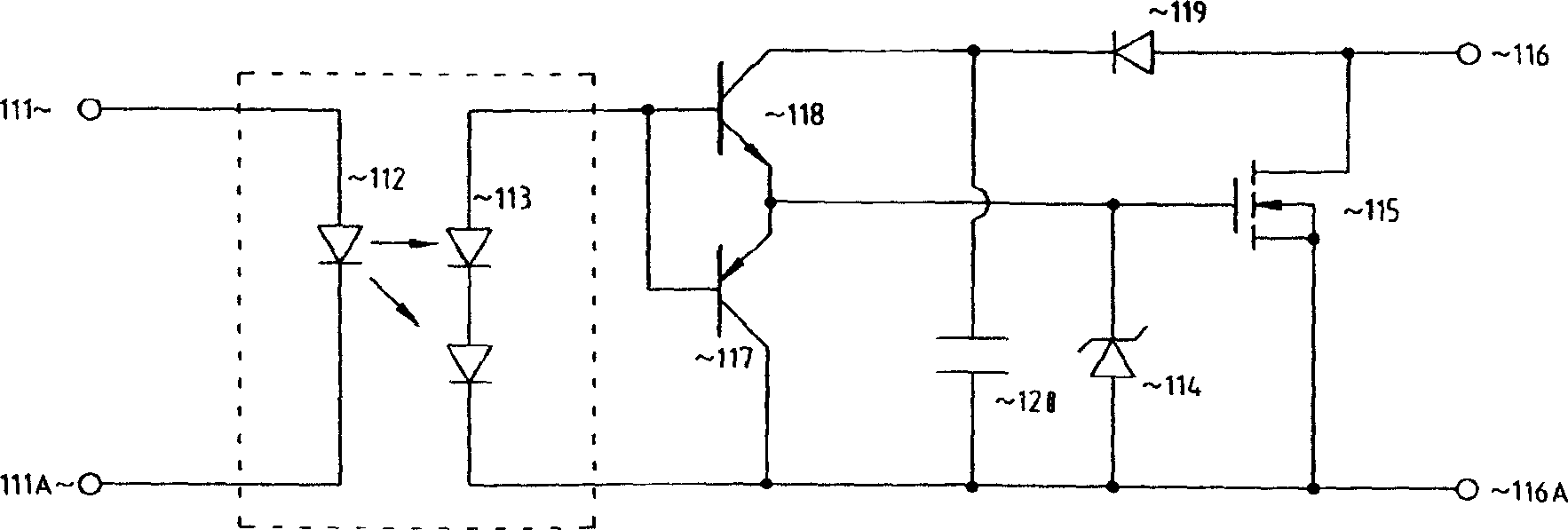
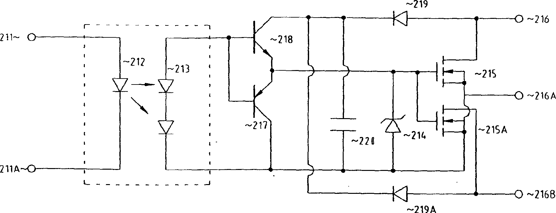
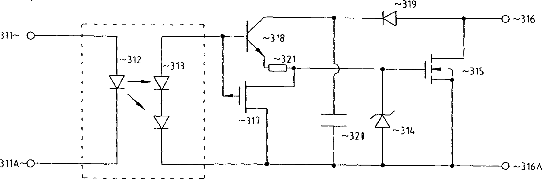
[0027] The present invention embodies the circuit structure of the high-speed switch normally open solid relay with the circuit diagram shown in the accompanying drawings. It includes: a light-emitting element that emits a light signal when receiving an input current; a photovoltaic diode array that generates a photovoltaic output when receiving a light signal from said light-emitting element; a normally-open metal oxide connected to the output of the relay field effect transistor. The present invention also includes a set of accelerated turn-on and accelerated turn-off circuits interposed between the photovoltaic diode array and the output metal oxide field effect transistor. When the photovoltaic diode array has photovoltaic output, the photovoltaic output is accelerated to turn on the circuit, the photogenerated voltage is coupled, and the photogenerated current is amplified and then applied to the gate and source of the output metal oxide field effect transistor. When the...


PUM


Abstract

The solid-state relay contains following parts: a luminous element; light voltaic diode array for generating effect of photoproduction voltage after receiving light signal; a field effect transistor (FET) for responding light voltaic output. The relay also includes a NPN triode and a PNP triode. Being connected to each other in parallel, base pole and emitter of the said triodes are connected between grids of light voltaic diode array and output FET. Base pole and emitter of the NPN triode as well as grid poles and source poles of light voltaic diode array and FET constitute series connection loop. A diode is inserted between collector of NPN triode and drain pole of FET. Cathode of the diode is connected to collector of NPN triode and a capacitor. The capacitor, NPN triode and diode constitute a charging circuit for grid of the FET. Being added in the invention, the charging and discharging circuit for grid of the FET quickens operation for turning on and off the solid-state relay.

Description

technical field [0001] The invention relates to a solid state relay. Background technique [0002] For example, the solid state relay (solid state relays English abbreviation SSR) rapid shutdown circuit introduced in US Patent No. 480486, "connect a control device to a photovoltaic diode array (photovoltaicdiode array English abbreviation PVDA) and an output metal oxide field effect transistor (power metal oxidesemiconductor field effect transistor English abbreviation MOSFET) between the gates, in order to be in a high impedance state when the photovoltaic output appears, and in a low impedance state when the photovoltaic output disappears, so that the charging current flows from the photovoltaic diode array to the output metal oxide field effect transistor gate". The control device described in the patent is an accelerated discharge circuit that outputs the gate charge of metal oxide field effect transistors, and uses various combinations of N-channel JFETs (normally clos...

Claims


Application Information

Patent Timeline
IPC IPC(8): H03K17/56H03K17/00
Inventor 李长寿曾志清杨延旭
Owner BEIJING KEYTONE ELECTRONICS RELAY
Why Eureka
Try Eureka