Ceramic electronic component and method for manufacturing the same

A technology of electronic components and manufacturing methods, applied in the direction of printed circuit manufacturing, electrical components, circuits, etc., can solve problems such as difficult to prevent, insufficient effect, and increased conduction resistance of via-hole conductors, so as to prevent voids and improve adhesion , The effect of stabilizing electrical characteristics

Inactive Publication Date: 2006-03-15
KYOCERA CORP
View PDF0 Cites 14 Cited by
  • Summary
  • Abstract
  • Description
  • Claims
  • Application Information

AI Technical Summary

Problems solved by technology

[0013] However, if the amount of inorganic particles contained in the conductive paste for via-hole conductors is large, the conduction resistance of the via-hole conductors 108 and 109 may increase, or the above-mentioned via-hole conductors 108 and 109 may be disconnected.
Therefore, the amount of inorganic particles contained in the conductive paste for via-hole conductors needs to be suppressed to a small amount. The effect of shifting the sintering star

Method used


Image

  • Ceramic electronic component and method for manufacturing the same
  • Ceramic electronic component and method for manufacturing the same
  • Ceramic electronic component and method for manufacturing the same

Examples


Embodiment Construction

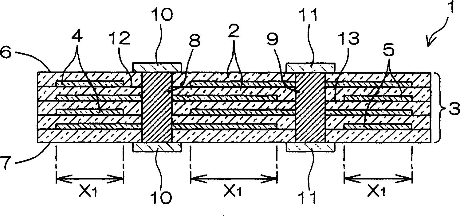
[0035] figure 1 It is a cross-sectional view showing a multilayer ceramic capacitor 1 as an example of the ceramic electronic component of the present invention. refer to figure 1 , The multilayer ceramic capacitor 1 of this example includes a dielectric block 3 in which a plurality of dielectric layers 2 formed of ceramics are stacked.

[0036] Between the layers of the respective dielectric layers 2 forming the dielectric block 3 , internal electrodes 4 and 5 serving as conductor wiring are alternately arranged for each of the plurality of layers. In addition, the dielectric block 3 is formed with via conductors 8, 9 extending from the upper surface 6 shown in the drawing to the lower surface 7 of the dielectric block 3 through its stacking direction, and the upper surface 6 and the lower surface 7 of the dielectric block 3 are , external electrodes 10 electrically connected to via-hole conductors 8 and external electrodes 11 electrically connected to via-hole conductors...


PUM


Abstract

The present invention relates to a ceramic electronic component wherein via conductors that are embedded in through holes of dielectric layers formed from a sintered body of ceramic particles are made by firing a electrically conductive paste for via conductor that contains inorganic particles made of the same material as the ceramic particles that constitute the dielectric layer and having an average particle diameter smaller than that of the ceramic particles, and a method for manufacturing the same. According to the present invention, such a ceramic electronic component can be provided that the via conductors and the internal electrodes are electrically connected with each other satisfactorily without voids generated therein.

Description

technical field [0001] The present invention relates to a ceramic electronic component including a dielectric layer formed of a sintered body of ceramic particles and provided with a through hole, a via conductor embedded in the through hole of the dielectric layer, and a method for manufacturing the ceramic electronic component. Background technique [0002] In recent years, in multilayer ceramic capacitors and the like, especially ceramic electronic components having a laminated structure with two or more laminated dielectric layers, in order to reduce the equivalent series resistance or equivalent series Inductance, and the use of a structure in which the above-mentioned conductor wiring is electrically connected to a via conductor penetrating through the stacking direction of the ceramic electronic component is gradually increasing. [0003] Figure 9 It is a cross-sectional view showing an example of the multilayer ceramic capacitor 101 having the above structure. refe...

Claims


Application Information

Patent Timeline
IPC IPC(8): H01G4/30H01B1/22
CPCH01G4/2325H05K1/092H05K3/4061H05K2201/0209
Inventor 佐藤恒
Owner KYOCERA CORP
Why Eureka
Try Eureka