Semiconductor device and manufacturing method thereof

A semiconductor and device technology, applied in the field of semiconductor devices and their manufacturing, can solve problems such as inability to provide transistor performance

Inactive Publication Date: 2006-03-22
DONGBUANAM SEMICON
View PDF1 Cites 7 Cited by
  • Summary
  • Abstract
  • Description
  • Claims
  • Application Information

AI Technical Summary

Problems solved by technology

However, for semiconductor devices on the order of less than 90 nm lines, nitride layers cannot be formed by such thermal nitridation because such thermal nitride layers cannot provide the desired transistor performance

Method used


Image

  • Semiconductor device and manufacturing method thereof
  • Semiconductor device and manufacturing method thereof
  • Semiconductor device and manufacturing method thereof

Examples


Embodiment Construction

[0029] Exemplary embodiments of the present invention will be described below with reference to the accompanying drawings.

[0030] The present invention is described with reference to the accompanying drawings so that those skilled in the art can practice the present invention. It will be apparent to those skilled in the art that the described embodiments may be modified in various ways without departing from the spirit of the invention as disclosed in the claims.

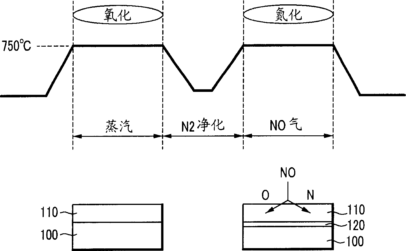
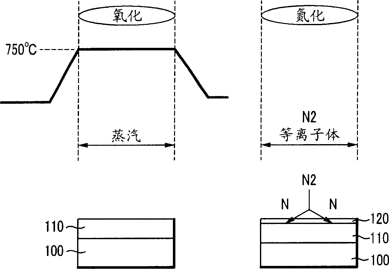
[0031] Figure 1A shows a method for thermally forming a nitride layer, Figure 1B A method for forming a nitride layer using plasma is shown. The nitriding method can be classified into a thermal nitriding method and a plasma nitriding method.

[0032] Also, depending on how water or steam is generated (H 2 O), the gate oxide forming method can be classified into a torch method and a water vapor generator (WVG for short) method. The WVG method can form a thinner oxide layer. In the flame method, water or ste...


PUM


Abstract

A method of manufacturing a semiconductor device includes forming a gate oxide layer on a substrate and forming a nitride layer on the surface of the oxide layer using nitrogen at a concentration of 9 to 11% as a plasma gas. With such scheme, the plasma nitridation method is used so that charge mobility can be preserved for an NMOS transistor and the boron penetration is prevented for a PMOS transistor in a semiconductor having a gate length of 100 nm or less.

Description

[0001] Related technologies and their cross-references [0002] This application claims priority and benefit from Korean Patent Application No. 10-2004-0074497 filed in the Korean Intellectual Property Office on September 17, 2004, the entire contents of which are hereby incorporated by reference. technical field [0003] The present invention relates to a semiconductor device and a method of manufacturing the same. Background technique [0004] Typically, in MOSFETs, the gate insulating layer includes a silicon oxide layer. As semiconductor devices become more highly integrated and their operating speeds increase, the gate insulating layer therein becomes thinner and thinner. Therefore, because the gate insulating layer is thin, boron permeation may sometimes occur between the gate electrode and the silicon substrate. Therefore, for a semiconductor device having a very thin line structure (for example, less than 0.18 μm), boron penetration from the gate electrode to the s...

Claims


Application Information

Patent Timeline
Patent Type & Authority Applications(China)
IPC IPC(8): H01L21/31H01L21/28H01L21/336H01L29/78
CPCH01L21/28202H01L21/18
Inventor 金载熙
Owner DONGBUANAM SEMICON
Why Eureka
Try Eureka