Double layer printed circuit board capable of implementing impedance control

A printed circuit board, impedance control technology, applied in the direction of printed circuits, printed circuits, printed circuit components, etc., can solve problems such as unreasonable, non-compliance with impedance matching, and failure to consider the requirements of transmission line 150 impedance control.

Inactive Publication Date: 2006-03-29
HONG FU JIN PRECISION IND (SHENZHEN) CO LTD +1
View PDF0 Cites 12 Cited by
  • Summary
  • Abstract
  • Description
  • Claims
  • Application Information

AI Technical Summary

Problems solved by technology

The thickness of the dielectric layer is 56mil. According to the above empirical formula, the characteristic impedance of the transmission line 150 is 150 ohms, which obviously does not meet the requirements of impedance matching. If the characteristic impedance of the transmission line 150 is to be equal to 60 ohms, according to the above empirical formula, W is the transmission line The wid

Method used


Image

  • Double layer printed circuit board capable of implementing impedance control
  • Double layer printed circuit board capable of implementing impedance control
  • Double layer printed circuit board capable of implementing impedance control

Examples


Embodiment Construction

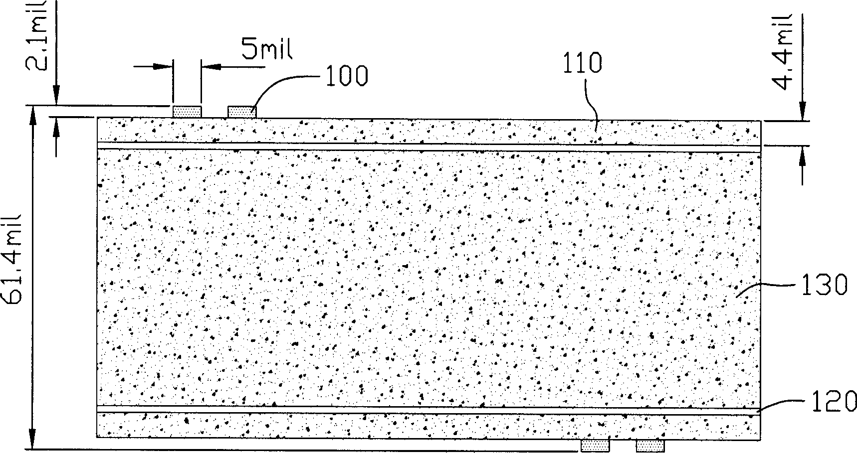
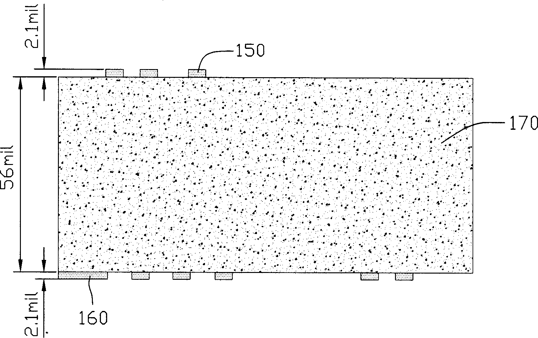
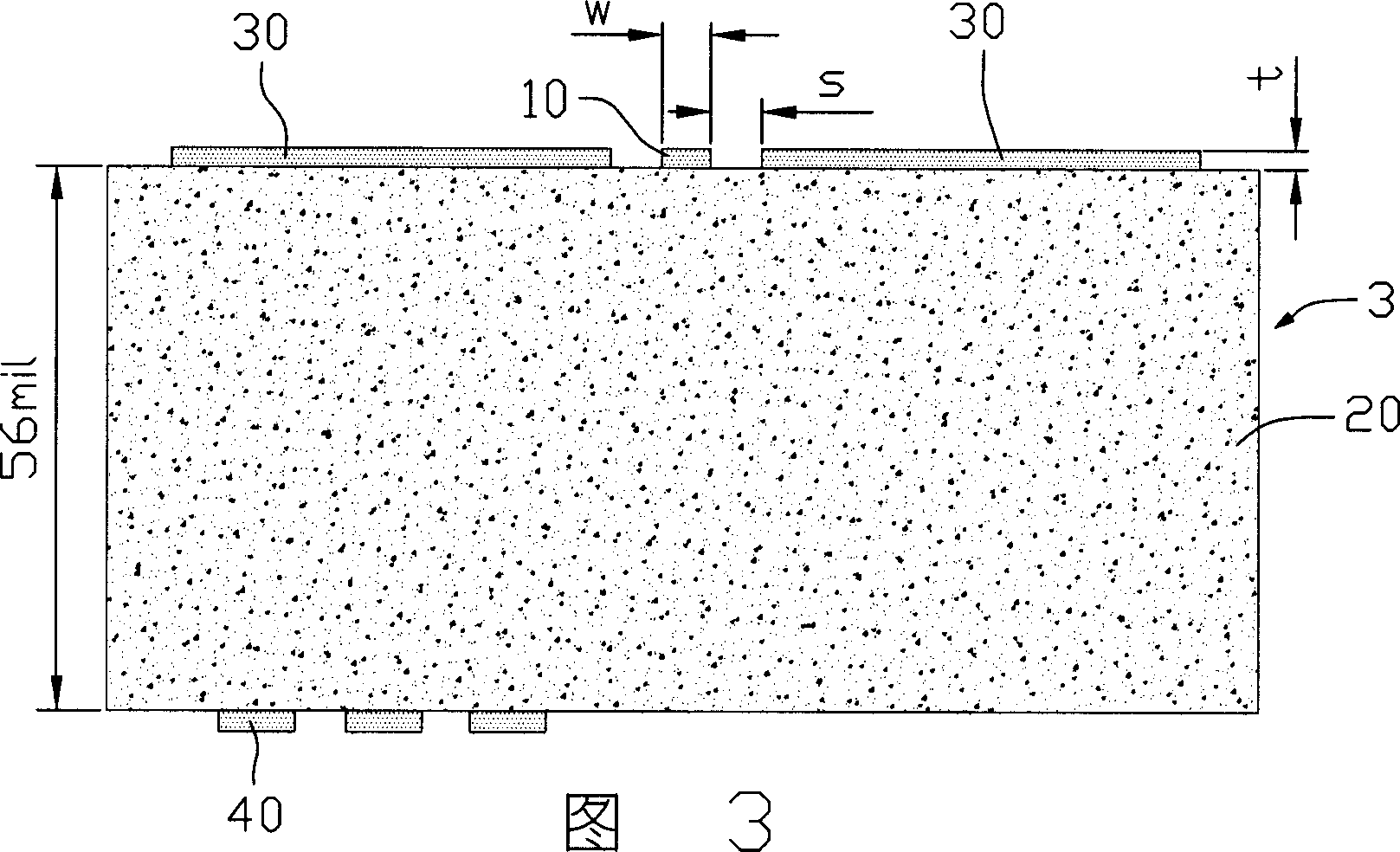
[0014] The present invention can realize the first embodiment of the two-layer printed circuit board of impedance control, as shown in Figure 3, two-layer printed circuit board 3 comprises several high-speed signal transmission lines (this embodiment is single-ended transmission line 10), a layer 20, several ground layers 30 and several low-speed signal lines 40. A grounding layer 30 is arranged on both sides of each single-ended transmission line 10. The grounding layer 30 and the single-ended transmission line 10 are arranged side by side on the dielectric layer 20. The thickness t of the grounding layer 30 is equal to the thickness t of the single-ended transmission line 10. The grounding layer 30 The length of is equal to the length of the single-ended transmission line 10. The width of the single-ended transmission line 10 is w, and the distance between each ground layer 30 and the single-ended transmission line 10 is s. To realize the impedance control of the single-end...


PUM


Abstract

A double-layer printed-circuit board capable of realizing the impedance control comprises a dielectric layer and several high-speed signal transmission lines and a ground plane adjacent to each high-speed signal transmission line on the dielectric layer. Using the said double-layer printed-circuit board can input the two-dimensional sectional graphic of the double-layer printed-circuit board to an artificial software. An ideal characteristic impedance value is obtained via the multiple adjustment of parameter value of the said high-speed signal transmission line and the relative location of the high-speed signal transmission line and the ground plane, the multiple input of the two-dimensional graphic and the multiple computation of the artificial software after comparing the characteristic impedance value of the high-speed signal transmission line counted by the artificial software and its standard impedance value.

Description

【Technical field】 [0001] The invention relates to a printed circuit board (Printed Circuit Board, referred to as PCB hereinafter), in particular to a two-layer printed circuit board capable of realizing impedance control in high-speed signal wiring. 【Background technique】 [0002] As the output switching speed of integrated circuits increases and the wiring density of PCB increases, signal integrity has become one of the issues that must be concerned in high-speed digital PCB design. Factors such as the parameters of components and PCB, the layout of components on PCB, and the wiring of high-speed signals will all cause signal integrity problems, resulting in unstable system operation, or even not working at all. How to fully consider the signal integrity factor in the PCB design process and take effective control measures has become a hot topic in the PCB design industry today. For transmission lines on PCBs, the most important thing to maintain signal integrity is impedan...

Claims


Application Information

Patent Timeline
IPC IPC(8): H05K1/00
CPCH01P3/08H05K1/0219H05K1/0245H05K1/0253H01P5/02H05K2201/09236
Inventor 许寿国白育彰
Owner HONG FU JIN PRECISION IND (SHENZHEN) CO LTD
Why Eureka
Try Eureka