Integrated circuit die connection methods and apparatus

a technology of integrated circuit and connection method, which is applied in the direction of electrical apparatus, semiconductor devices, semiconductor/solid-state device details, etc., can solve the problems of undetectable high impedance of bond wire, difficulty in connecting to a die, and difficulty in high-frequency connections, etc., to achieve easy controllable impedance, reduce bond wire length, and low cost

Inactive Publication Date: 2008-06-24
INTEL CORP
View PDF8 Cites 13 Cited by
  • Summary
  • Abstract
  • Description
  • Claims
  • Application Information

AI Technical Summary

Benefits of technology

[0010]Embodiments of this method provide a number of advantages, including a relatively low cost method of providing a reduction in bond wire length. Other embodiments of the method additionally or alternatively provide rf signal paths having a more readily controllable impedance, and a reduction in the number of layers required for the package substrate. Preferably the majority or substantially all of the analogue rf / microwave connections are made through the intermediate substrate; the digital circuitry may be directly connected to the substrate in a conventional manner, for example by wirebonding, tape automated bonding (TAB) or the like.
[0011]In preferred embodiments of the method the intermediate substrate is mounted on the package substrate such that a height above the package substrate of a portion of the intermediate substrate to which an rf bond pad connects substantially matches a height of the bond pad above the package substrate when the die is mounted on the package substrate (the method generally including mounting the die on the package substrate). Preferably therefore (depending upon how the intermediate substrate is mounted on the package substrate) a height or thickness of the intermediate substrate approximately matches a height or thickness of the die. Preferably the intermediate substrate is substantially adjacent the die to minimise bond wire length.
[0012]Preferably the intermediate substrate is configured to provide a controlled impendence pathway from an rf bond pad to a substrate pad, preferably along substantially the whole length of such a connection. For example, in one embodiment a bond pad connection may be taken down through a via to the underside of the intermediate substrate (that is to the surface of the intermediate substrate closest to the package substrate) and then run along a track on this surface to a connection to a substrate pad, this environment for the track being more readily characterisable than that of an upper side of the intermediate substrate over which glob top will be applied. In other embodiments the intermediate substrate has three or more (conducting) layers so that a track may be run within the intermediate substrate, particularly preferably adjacent a ground plain or between a pair of ground plains. In this way the rf tracks may be effectively configured as transmission lines. It will be appreciated that the intermediate substrate need not provide a connection all the way from a die bond pad to a substrate pad it is preferable that at least the majority of the track length, more preferably substantially all the track length, is implemented in the intermediate substrate for improved impendence control. Furthermore, this allows a cheaper two layer package substrate to be used rather than the four layer substrate which would otherwise be needed (to provide ground planes).
[0013]Preferably the intermediate substrate is formed from a fired aluminia ceramic, but one particularly preferred material is LTCC (low temperature co-fired ceramic), which has low tan δ losses and a high and well-controlled dielectric constant, which facilitates thinner tracks of well-characterised impedance. However other materials such as HTCC (high temperature co-fired ceramic) or glass fibre-based materials such as FR4 may also be employed.
[0014]Preferably embodiments of the method include shaping the intermediate substrate so that a portion of its perimeter substantially matches a portion of the perimeter of the die. In particular, since there is generally a great deal more digital than rf circuitry the die may be configured so that the rf circuitry occupies one corner of the die, in which case the intermediate substrate can be shaped so that it fits around this corner of the die (i.e. approximately L-shaped). This leaves a portion of the perimeter of the die available for making conventional wire bonded connections from the package substrate directly to bond pads for the digital circuitry. Fabricating the intermediate substrate from co-fired ceramic facilitates this shaping process since the material prior to firing (“green tape”) may simply be stamped or punched in to the desired shape, which is much cheaper than, say, the milling procedure which would be needed for glass fibre. Using LTCC facilitates the fabrication of tracks from low (ohmic) loss materials such as gold or silver (for HTCC materials the more resistive tungsten would generally be needed).
[0017]Preferably substantially all the first contacts are adjacent a periphery of the intermediate substrate, to minimise the rf wirebonding distance required. Generally the first contacts will comprise wirebonding pads but a range of technologies is available for the second contacts including metal (for example solder or gold) bumps or balls and off-surface leads, pins, springs or the like. Preferably the second contacts provide a degree of compliance to allow for a co-efficient of thermal expansion mismatch between the intermediate substrate and the package substrate. Metal pins (as described later) are particularly preferable as they are also able to space the intermediate substrate away from the package substrate a distance approximately equal to the thickness of the adhesive attaching the die (meniscus height) so that the heights of the intermediate substrate and die substantially correspond, although other means may also be employed to achieve this.

Problems solved by technology

Wirebonding techniques, although relatively popular and inexpensive, suffer from problems at higher frequencies, in particular microwave frequencies above 1 GHz because of the bond wire inductance.
This can result in the bond wire having an undesirably high impedance at these frequencies.
The π filter ofFIG. 1c produces a low pass response with a typical cut-off frequency in the range 1 GHz to 10 GHz, which is a problem for many single chip mixed signal (digital and rf) devices, particularly as the rf operating frequencies increase above 1 GHz.
It is desirable to be able to reduce the length of a bond wire 16 to reduce the inductance and hence push the low pass filter cut off frequency above the relevant band of interest, but conventional methods of connecting to a die make this difficult.
It is known to mount a microwave integrated circuit in a cavity on a ceramic substrate to reduce the length of the bond wires, but this is expensive.
Another approach is to separate the rf and digital circuitry into two separate chips, but this has the disadvantage of requiring many connections between the two chips, which is expensive.

Method used


Image

  • Integrated circuit die connection methods and apparatus
  • Integrated circuit die connection methods and apparatus
  • Integrated circuit die connection methods and apparatus

Examples


Embodiment Construction

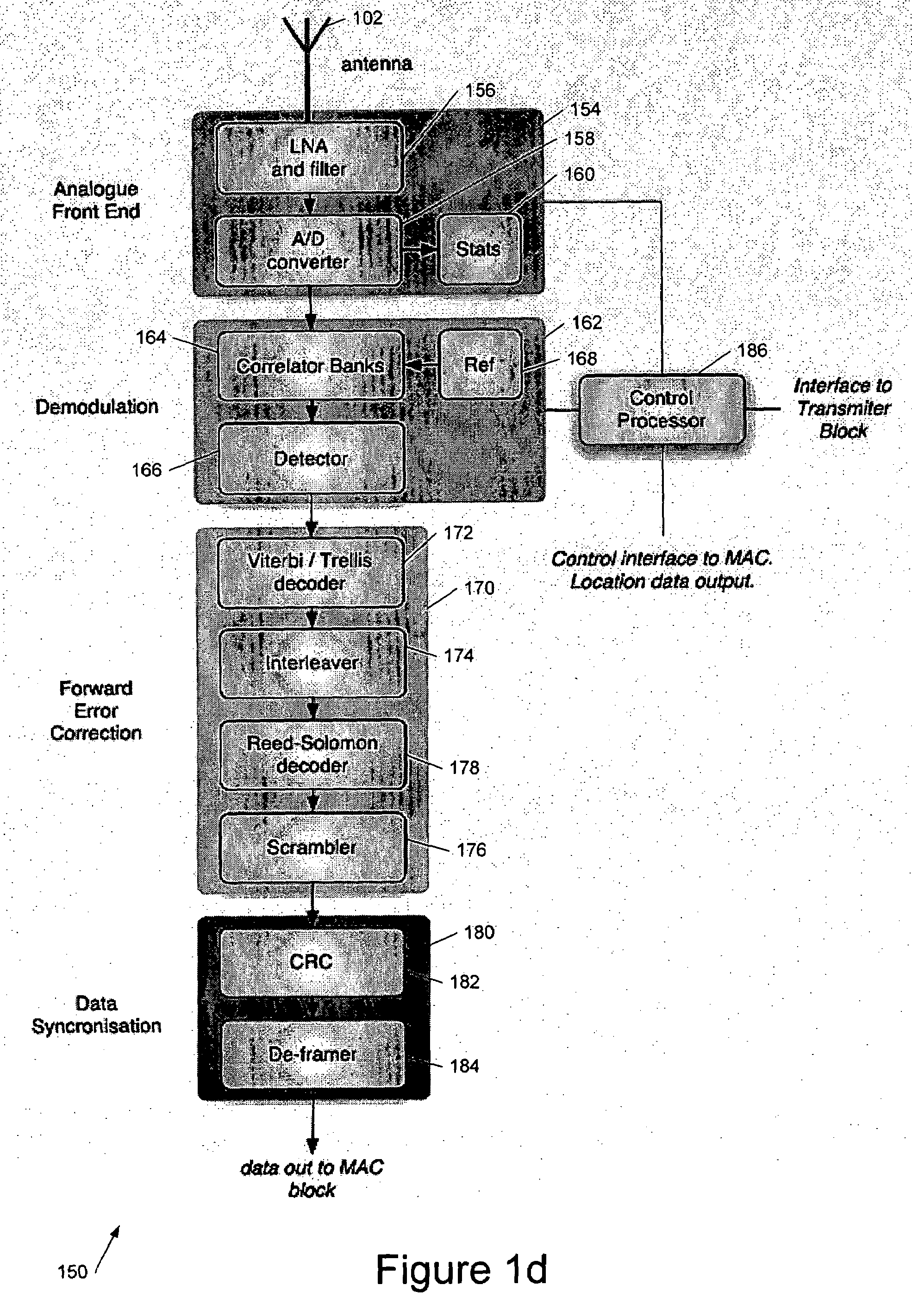
[0028]Some preferred embodiments of the invention are useful for connecting to a die for a single chip mixed signal (analogue rf and digital) monolithic device, in particular for a UWB (ultra wideband) receiver, transmitter or transceiver chip. An example of such a device will therefore be briefly outlined with reference to FIG. 1d, which shows a block diagram of a UWB receiver 150.

[0029]An incoming UWB signal is received by (off-chip) antenna 102 and provided to analog front end block 154 which comprises a low noise amplifier (LNA) and filter 156, and an analogue-to-digital converter 158. A set of counters or registers 160 is also provided to capture and record statistics relating to the received UWB input signal. The analog front end 154 is primarily responsible for converting the received UWB signal into digital form.

[0030]The digitised UWB signal output from front end 154 is provided to a demodulation block 162 comprising a correlator bank 164 and a detector 166. The digitised i...


PUM


Abstract

This invention generally relates to methods and apparatus for connecting to an integrated circuit die, in particular where the die includes both analogue / microwave radio frequency (rf) circuitry and digital circuitry. A method of connecting a die having both microwave radio frequency (rf) circuitry and digital circuitry to a substrate of a package for the die, the die having a plurality of bond pads, some for said rf circuitry and some for said digital circuitry, the substrate having a plurality of interconnects for making external connections to said package and a plurality of substrate pads for connecting said interconnects to said die, the method comprising: connecting at least one of said bond pads for said rf circuitry to a substrate pad by connecting said rf bond pad to an intermediate substrate and connecting said intermediate substrate to said substrate pad. Preferably at least some of the bond pads for the digital circuitry are directly connected to the substrate pads, for example by wire bonding.

Description

BACKGROUND OF THE INVENTION[0001]1. Field of the Invention[0002]This invention generally relates to methods and apparatus for connecting to an integrated circuit die, in particular where the die includes both analogue / microwave radio frequency (rf) circuitry and digital circuitry.[0003]2. Background Art[0004]One of the commonest methods of making connections from an integrated circuit die to an underlying package substrate bearing external interconnects for the integrated circuit is by means of wirebonding. With this technique a fine bond wire, typically of gold or aluminium, is used to connect a pad on the die to a pad on the package (or interconnect) substrate.[0005]FIGS. 1a and 1b show a vertical cross-section and a view from above of a typical wirebonded integrated circuit 10 in which the die 12 is mounted on a ball grid array (BGA) substrate 14. Die pads 12a are connected to substrate pads 14a by means of a plurality of wirebonds 16 (omitted for clarity in the view from above),...

Claims


Application Information

Patent Timeline
Patent Type & Authority Patents(United States)
IPC IPC(8): H01L21/50H01L21/44H01L23/34H01L23/48H01L23/52H01L23/40H01L21/48H01L23/13H01L23/15H01L23/49H01L23/498H01L23/66
CPCH01L23/13H01L23/49811H01L23/49816H01L23/49827H01L23/49833H01L23/66H01L24/48H01L23/15H01L24/28H01L24/45H01L2223/6611H01L2224/16225H01L2224/2919H01L2224/32225H01L2224/45014H01L2224/45015H01L2224/45124H01L2224/45144H01L2224/48011H01L2224/48091H01L2224/48137H01L2224/48227H01L2224/48472H01L2224/48599H01L2224/48699H01L2224/49111H01L2224/49175H01L2224/73257H01L2224/73265H01L2924/01005H01L2924/01013H01L2924/01014H01L2924/01018H01L2924/01027H01L2924/01028H01L2924/01029H01L2924/01031H01L2924/01047H01L2924/01057H01L2924/01074H01L2924/01079H01L2924/014H01L2924/04953H01L2924/09701H01L2924/10329H01L2924/14H01L2924/15311H01L2924/20752H01L2924/30107H01L2924/3011H01L2924/00014H01L2924/0665H01L24/49H01L2924/01006H01L2924/01087H01L2924/00012H01L2924/00H01L2924/15787H01L2224/85207H01L24/73H01L2924/00015H01L2224/85399H01L2224/05599H01L2924/206H01L23/12H01L23/48H01L23/50H01L23/49
Inventor ELLWOOD, STEPHEN
Owner INTEL CORP
Why Eureka
Try Eureka