Wafer measuring system

A technology for measuring systems and wafers, applied in the fields of high-frequency components, circuit components and system functions, can solve the problems of occupying space, difficult to provide the shock-proof function of the probe machine at the same time, signal strength loss, etc.

A technology for measuring systems and wafers, applied in the fields of high-frequency components, circuit components and system functions, can solve the problems of occupying space, difficult to provide the shock-proof function of the probe machine at the same time, signal strength loss, etc.

CN1755910AActive Publication Date: 2006-04-05RICHWAVE TECH CORP

Image

  • Wafer measuring system
  • Wafer measuring system
  • Wafer measuring system

Examples


Embodiment Construction

[0042] The preferred embodiments of the present invention are described in detail below in conjunction with the accompanying drawings, but these descriptions are only used to illustrate the present invention, rather than to limit the scope of rights of the present invention.

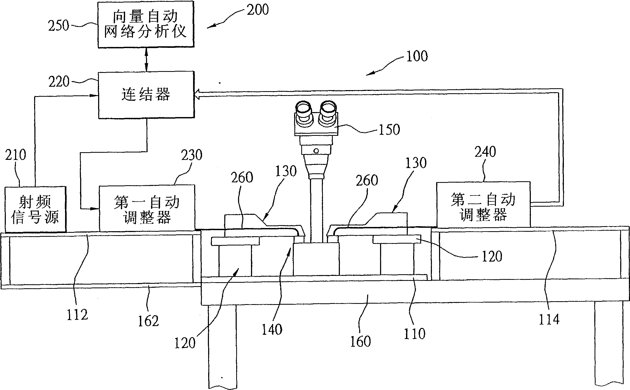
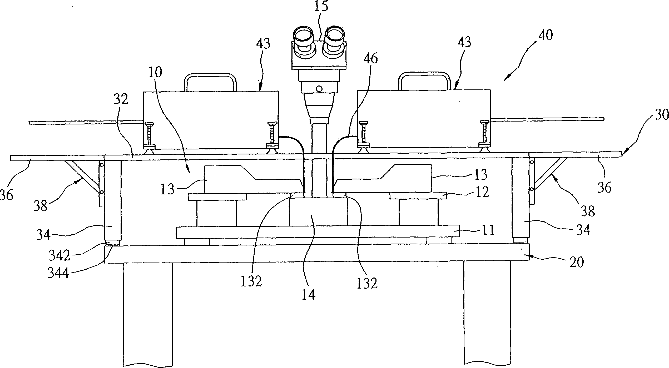
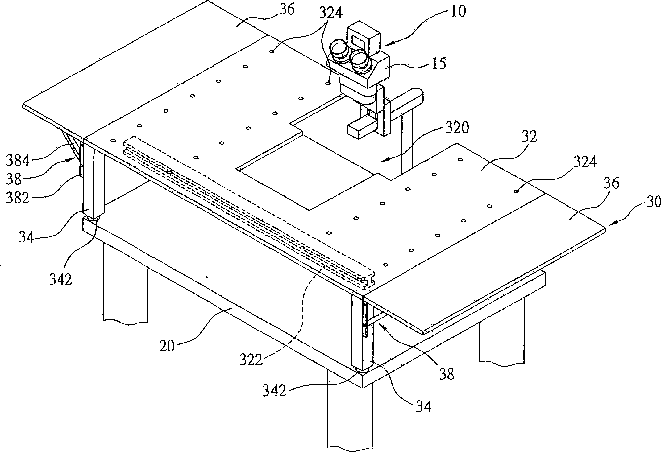
[0043] see figure 2 and image 3 , are respectively the front view of the wafer measurement system of the present invention and the perspective view of the carrying device of the present invention. The wafer measurement system provided by the present invention includes a probe machine 10 , a shockproof table 20 , a carrying device 30 , and a high-frequency measurement device 40 .

[0044] The probe machine 10 includes a base 11 , a probe platform 12 , a pair of probe holders 13 , a wafer holder 14 , and a microscopic observation device 15 . The probe platform 12 is placed on the base 11; the pair of probe supports 13 are respectively placed on both sides of the probe platform 12; the wafer holder 14 is...


PUM


Abstract

The invention relates to a crystal measurement system for providing a improved supporting device and reducing the space possessed by measurement machine. Said crystal measurement system comprises a feeling spindle table, a supporting device, and a high-frequency measurement device. Wherein, the feeling spindle stable comprises a base, a feeling spindle platform, a couple of feeling spindle brackets arranged on the two sides of feeling spindle platform, a crystal clamp base between said couple feeling spindle brackets and a micro-observing device; the supporting device comprises a rigid plate over the feeling spindle bracket and several posts, while the rigid plate has a concave cut to be observed by micro-observing device; and the high-frequency measurement device at least comprises a automatic regulator arranged on the rigid plate and a signal connecting line through said concave cut and connecting the automatic regulator and the feeling spindle bracket.

Description

technical field [0001] The invention relates to a wafer measurement system, in particular to a measurement system using high-frequency measurement technology to detect high-frequency components, circuit components and system functions in the wafer. Background technique [0002] Due to the rapid development of communication products and communication systems, no matter in wireless communication, wired communication or optoelectronics, they are booming. Among them, related semiconductor integrated circuits are currently key research and development projects in related fields, especially in the rapid development of high-frequency communication, and a large amount of resources are actively invested in the development and design of related circuits, processes, components, etc. However, these related developments and designs ultimately require high-frequency measurement. High-frequency measurement technology can be used to verify whether the high-frequency components, circuit comp...

Claims


Application Information

Patent Timeline
05 Apr 2006
Publication
CN1755910A
IPC
H01L21/66; G01R31/26; G01R31/28
Inventors
吴经国; ηŽ‹ζ˜―η¦