Supercharge Your Innovation With Domain-Expert AI Agents!

Image processing method for low light level

An image processing, low illumination technology, applied in the field of image processing, can solve the problems of occupation, complex calculation process, multi-system resources, etc.

Inactive Publication Date: 2006-04-19
MITAC COMP (SHUN DE) LTD +1
View PDF0 Cites 0 Cited by
  • Summary
  • Abstract
  • Description
  • Claims
  • Application Information

AI Technical Summary

Problems solved by technology

Please refer to figure 1 After the image 100 is focused by a lens 110, it is projected on a CMOS image sensor 120, and the obtained image is processed by a digital signal processor (DSP) 130 and a central processing unit (CPU) 140 at the back end, Therefore, the quality of the image is better, but because the calculation process of the signal processor 130 is relatively complicated, it takes up too many system resources
In addition, on the PDA, no signal processor is used, but the image obtained by the CMOS image sensor is converted by an analog / digital converter (ADC), and the analog signal is converted into a digital signal for the central processing unit (CPU) to display. image, so the picture quality will be affected
Therefore, although the CMOS image sensor will have good image quality under normal illumination, the quality effect under low illumination is still not good.

Method used


Image

  • Image processing method for low light level
  • Image processing method for low light level
  • Image processing method for low light level

Examples


Embodiment Construction

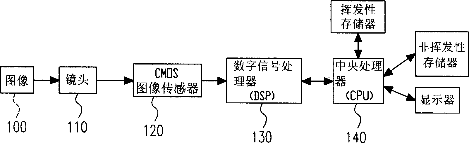
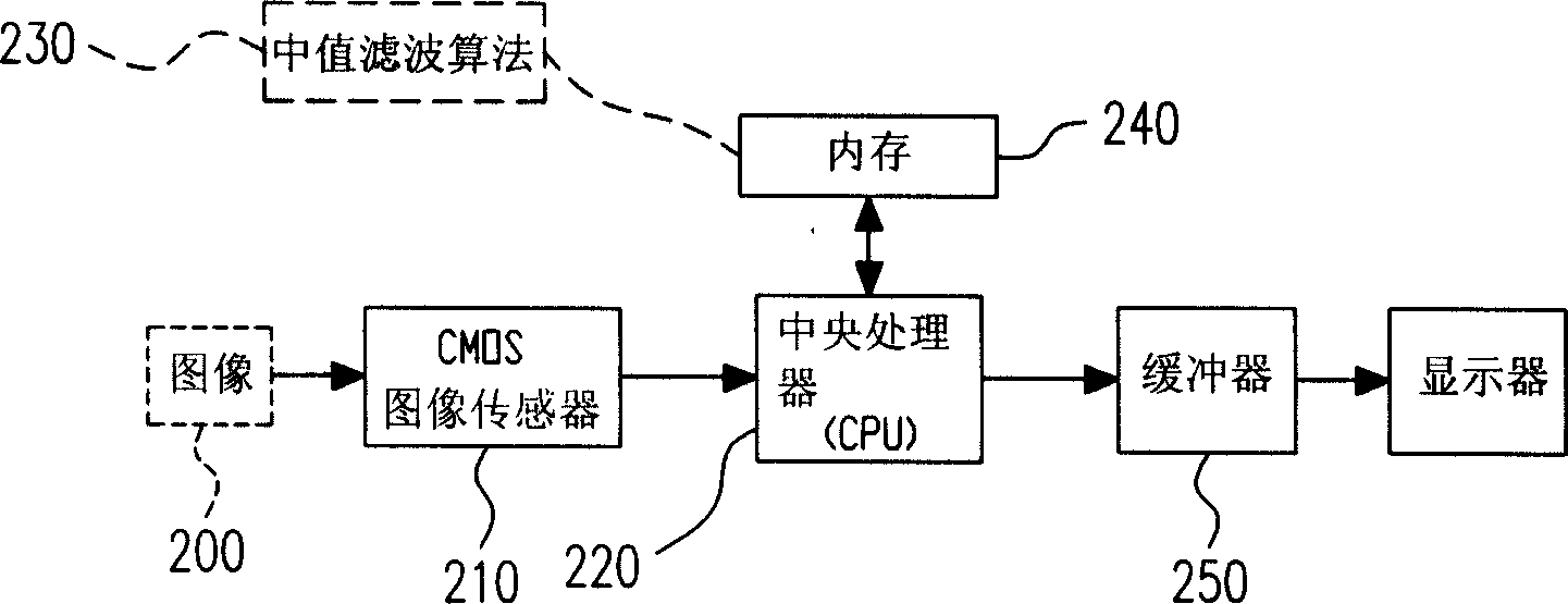
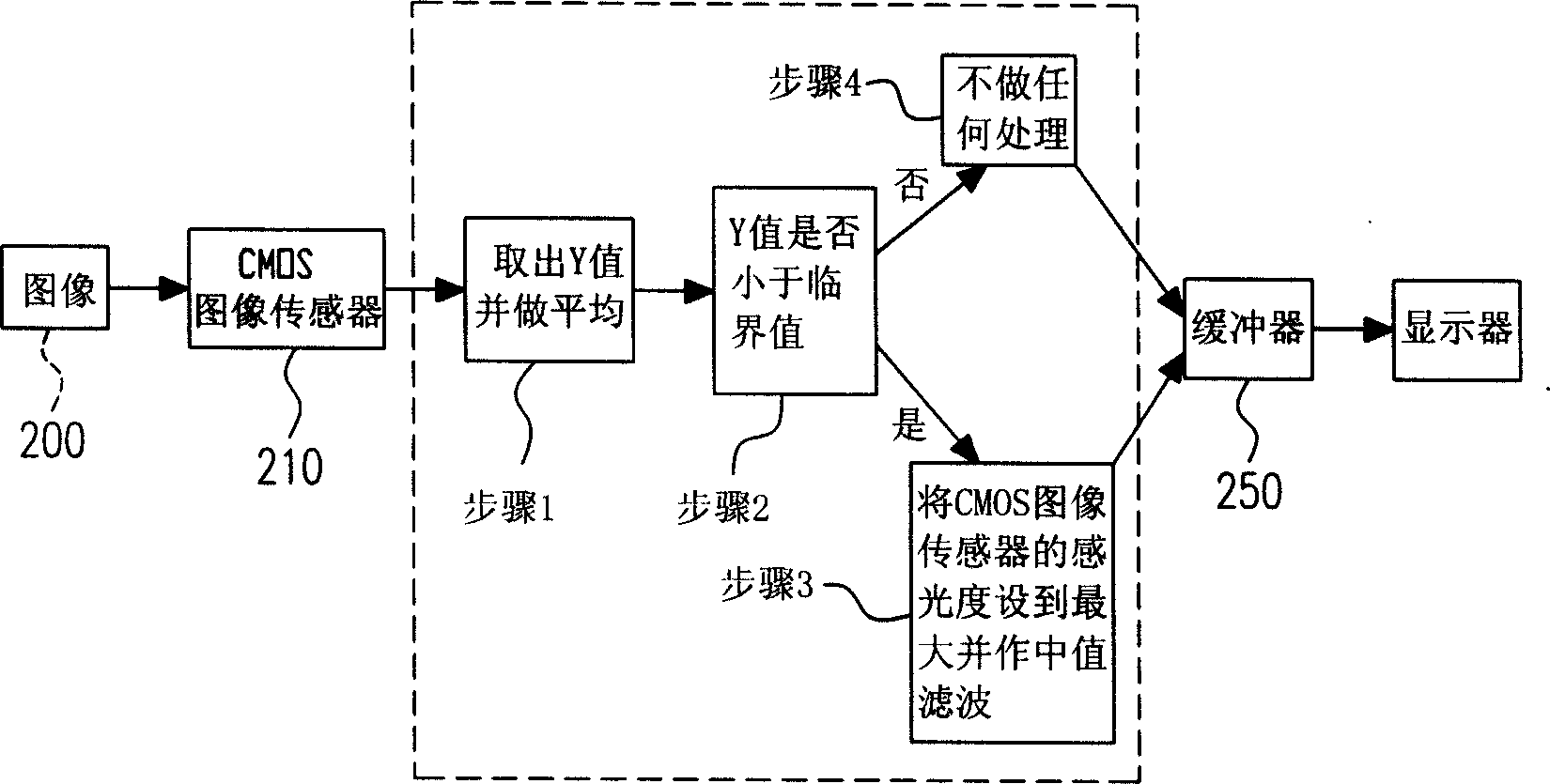
[0013] Please refer to figure 2 , which is a flow block diagram of a low-illuminance image processing method in a preferred embodiment of the present invention, which is suitable for a CMOS image sensor. Under normal illumination conditions, such as daytime photography, or obtaining images in well-lit places such as outdoor suburbs, the CMOS image sensor 210 has good image quality, but under low illumination conditions, such as nighttime photography, or insufficient indoor lighting, etc. In the case of dim light, the effect of the image is not good, and even noise may occur, which affects the quality of the image. Since the CMOS image sensor 210 has noise only under low illumination conditions, the present invention calculates the average brightness value of an image 200 to determine that low illumination conditions are used for image processing.

[0014] Please refer to figure 2 After the CMOS image sensor 210 obtains an image 200, a central processing unit 220 can be use...


PUM


Abstract

The method is suitable CMOS image sensor. When mean brightness value of image is lower than noise critical value of CMOS image sensor, the method removes noise of CMOS image sensor by using median filtering algorithm. Advantages are: not complex calculation procedure so as to use not many system resources, suitable to process image in real time. CMOS image sensor provides good processing quality of image in high illumination and low illumination.

Description

【Technical field】 [0001] The present invention relates to an image processing method, and in particular to a low-illuminance image processing method. 【Background technique】 [0002] With the vigorous development of communications and digital technology, it has become a trend to pair electronic products such as PDAs, Pocket PCs, Portable PCs and Mobile Phones with digital cameras. . Generally speaking, image sensors can be mainly classified into two types: Charge Coupled Device (CCD) and Complementary Metal Oxide Semiconductor (CMOS). Both go through the same photoelectric conversion process that converts image incident light into electrical voltage. Based on power-saving and low-cost considerations, the use of charge-coupled devices (CCD) is expensive due to the special manufacturing process, and the drive circuit must operate at a high voltage so that the power consumption is high. On the contrary, CMOS image sensors have power-saving and easy-to-use The advantages of pe...

Claims


Application Information

Patent Timeline
Patent Type & Authority Applications(China)
IPC IPC(8): H04N5/235H01L27/148H04N5/225
Inventor 侯匡叡
Owner MITAC COMP (SHUN DE) LTD
Features
  • R&D
  • Intellectual Property
  • Life Sciences
  • Materials
  • Tech Scout
  • Unparalleled Data Quality
  • Higher Quality Content
  • 60% Fewer Hallucinations
Learn More