Multilayer printed wiring board-use copper-clad laminate sheet, multilayer printed wiring board and production method for multilayer printed wiring board

A multi-layer printing and wiring board technology, applied in printed circuit manufacturing, multi-layer circuit manufacturing, printed circuit, etc., can solve the misalignment of inner layer circuit, unevenness of single-sided circuit substrate, film thickness or stickiness of adhesive layer Differences and other issues

Inactive Publication Date: 2006-05-24
MATSUSHITA ELECTRIC WORKS LTD
View PDF1 Cites 6 Cited by
  • Summary
  • Abstract
  • Description
  • Claims
  • Application Information

AI Technical Summary

Problems solved by technology

[0007] However, in the technical solution disclosed in Patent Document 2, an adhesive layer is formed on the surface of the insulating rigid substrate on which the circuit is formed and opposite to the circuit, but it is intended to form an insulating rigid substrate on one side of the circuit. When the surface opposite to the circuit is coated with an adhesive and then heated, or the adhesive sheet is laminated while heating to form an adhesive layer, there is a partial difference in heat capacity depending on whether there is a circuit on the back side, and as a result , resulting in partial differences in the film thickness or viscosity of the adhesive layer
[0008] In particular, when the insulating hard substrate is thin, there is a problem that partial variations occur when the adhesive is formed, thereby causing partial variations in the film thickness or viscosity of the adhesive layer, In this case, the obtained single-sided circuit board with the adhesive layer is warped or distorted, and it is remarkably difficult to align a plurality of these single-sided circuit boards when they are stacked, heated and pressurized.
[0009] In addition, even if the positions of multiple single-sided circuit boards are stacked and aligned by the pin lamination method, the single-sided circuit board will become uneven as long as warpage or misalignment occurs on the single-sided circuit board. There is a problem that the position of the inner layer circuit is misaligned in the multilayer printed wiring board obtained by pressing

Method used


Image

  • Multilayer printed wiring board-use copper-clad laminate sheet, multilayer printed wiring board and production method for multilayer printed wiring board
  • Multilayer printed wiring board-use copper-clad laminate sheet, multilayer printed wiring board and production method for multilayer printed wiring board
  • Multilayer printed wiring board-use copper-clad laminate sheet, multilayer printed wiring board and production method for multilayer printed wiring board

Examples


Embodiment 1

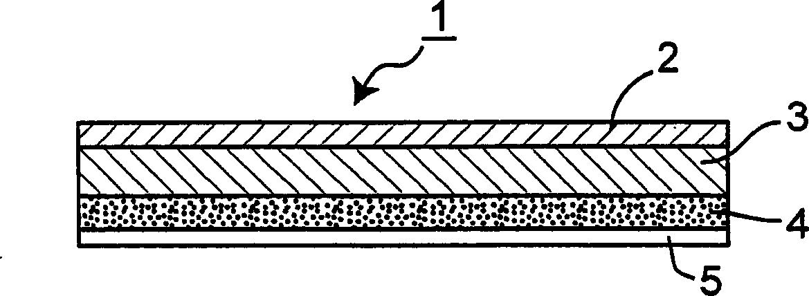
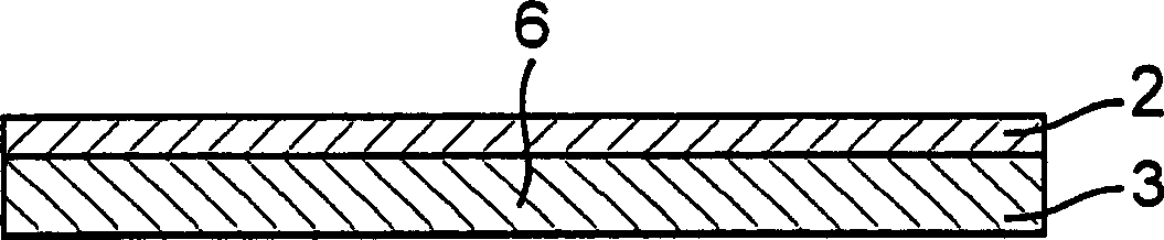
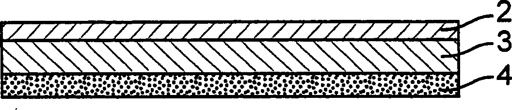
[0076] As such Figure 2A The single-sided circuit board 6 shown uses FR-4 grade glass fabric base epoxy resin single-sided copper foil laminated board (manufactured by Matsushita Electric Works, product number R-1661, with a thickness of 0.1mm in hard insulating layer, The thickness of the copper foil is 18μm). Secondly, such as Figure 2B As shown, an epoxy resin adhesive is applied to the surface of the hard insulating layer 3 with a thickness of 30 μm by roll coating, and heated (60° C.) until there is no tuck property to form the adhesive layer 4. Next, using a laminator (temperature 80°C, pressure 0.05MPa), the protective film 5, namely, a polyethylene terephthalate film (manufactured by Toray Corporation, product number T-60, thickness 38μm) was laminated on the adhesive The surface of the adhesive layer 4, such as Figure 2C As shown, a copper foil laminated board 1 for a multilayer printed wiring board is manufactured.

[0077] Next, a photosensitive dry film is laminated...

Embodiment 2

[0083] Same as in Example 1, manufactured as Figure 5 The single-sided circuit boards 11a, 11b, 11c, and 11d are shown. Secondly, the upper and lower surfaces of the core substrate 13 that are connected between the inner circuits formed on both sides, such as Figure 5 As shown, the single-sided circuit boards 11a, 11b and the single-sided circuit boards 11c, 11d are respectively arranged, and pseudo-fixed and aligned in position by the pin lamination method. The single-sided circuit boards 11a, 11b, 11c, and 11d are flat surfaces on which no warpage or distortion occurs. Therefore, the position can be easily aligned.

[0084] In this way, after overlapping and aligning the core substrates 13 and the single-sided circuit substrates 11a, 11b, 11c, and 11d, they are heated and pressurized (180°C, 1 hour) under vacuum using hot pressing to obtain Figure 6 The multilayer printed wiring board 12 is shown. The obtained multilayer printed wiring board 12 did not cause misalignment in t...

Embodiment 3

[0086] Same as in Example 1, manufactured as Figure 7 Single-sided circuit boards 11b and 11c are shown. In addition, such as Figure 7 As shown, the conductive bumps 10 are formed, and the surface layer substrate 14a with no circuit formed on the copper-clad foil 2 was manufactured under the conditions for manufacturing the single-sided circuit board 11a in Example 1. Similarly, another surface layer substrate 14b was manufactured.

[0087] Secondly, such as Figure 7 As shown, the surface layer substrate 14a, the single-sided circuit substrates 11b, 11c, and the other layer substrates 14b are superimposed and aligned, and the positions are pseudo-fixed by the lamination method. The surface-layer substrates 14a, 14b, and the single-sided circuit boards 11b, 11c are flat surfaces on which no warpage or distortion occurs, and therefore, position alignment is easy.

[0088] In this way, after the surface layer substrates 14a, 14b, and the single-sided circuit substrates 11b, 11c ar...


PUM

PropertyMeasurementUnit
surface roughnessaaaaaaaaaa
thicknessaaaaaaaaaa
heightaaaaaaaaaa

Abstract

A multilayer printed wiring board and its manufacturing method, by using a copper foil laminated board (1) for a multilayer printed wiring board to manufacture a multilayer printed wiring board so that a plurality of single-sided sheets with an adhesive layer are stacked and aligned The positional alignment of the circuit board becomes easy, thereby providing a multilayer printed wiring board and a manufacturing method thereof capable of reducing the occurrence of misalignment defects. Among them, the multilayer printed wiring board is composed of a copper-clad foil (2) that does not form a circuit, a hard insulating layer (3) formed by curing a thermosetting resin, and an adhesive layer (4) that can be temporarily melted by heating. It is integrated with the protective film (5) in this order.

Description

Technical field [0001] The present invention relates to a copper-clad laminate sheet for a multilayer printed wiring board (copper-clad laminatesheet), a multilayer printed wiring board, and a method for manufacturing a multilayer printed wiring board. Specifically, it relates to interstitial via hole A copper foil laminated board for a multilayer printed wiring board useful in the manufacture of a multilayer printed wiring board with a) structure, and a multilayer printed wiring board manufactured using the copper foil laminated board for a multilayer printed wiring board, and a manufacturing method thereof . Background technique [0002] The method of manufacturing a multilayer printed wiring board with a gap via structure has been studied for a long time (see, for example, Patent Document 1). In recent years, laser processing technology and solder paste printing technology have been advancing rapidly, and there has been proposed a technical solution that can reduce the number ...

Claims


Application Information

Patent Timeline
Patent Type & Authority Applications(China)
IPC IPC(8): B32B5/28H05K3/46B32B15/08H05K3/38H05K3/40
CPCH05K3/4655H05K3/386H05K3/4069H05K3/4617H05K3/4626H05K3/4652H05K2201/0129H05K2201/0195
Inventor 金谷大介前田修二福井太郎
Owner MATSUSHITA ELECTRIC WORKS LTD
Why Eureka
Try Eureka