
Method and system for imaging interference photoetching adopting white laser

An imaging interference and lithography system technology, applied in microlithography exposure equipment, photolithography process exposure devices, electrical components, etc., can solve problems such as poor image quality and low exposure efficiency, achieve good stability and improve exposure efficiency. , the simple effect of interference lithography

Inactive Publication Date: 2006-06-14
INST OF OPTICS & ELECTRONICS - CHINESE ACAD OF SCI
View PDF0 Cites 6 Cited by
  • Summary
  • Abstract
  • Description
  • Claims
  • Application Information

AI Technical Summary

Problems solved by technology

[0002] Imaging interference lithography is a new lithography technology, which can realize the high resolution of interference lithography and the ability of traditional optical lithography to generate arbitrary graphics. The general imaging interference lithography method is a three-exposure method, and the general The imaging interference lithography system consists of lasers, beam expanders, filtering and collimation systems, beam splitters, masks, imaging systems and resist substrates, etc., document S.R.J.Brueck, Imaging Interferometric Lithography, Microlithography World, Winter 1998, 2 -11 and literature Xiaolan Chen and S.R.J.Brueck, Imaging Interferometric Lithography: A Wavelength Division Multiplex Approach to Extending Optical Lithography, J.Vac.Sci.Technol, B16(6): 3392-3397, Nov / Dec.1998 Introduced imaging interferometric light The principle and general method of lithography technology, but the implementation method and system of imaging interference lithography are less discussed. The method in the literature is to use one wavelength for three exposures, and adjust the optical path between exposures to achieve exposure of different spatial frequency components. , there are problems such as pattern alignment, poor image quality and low exposure efficiency

Method used


Image

  • Method and system for imaging interference photoetching adopting white laser
  • Method and system for imaging interference photoetching adopting white laser
  • Method and system for imaging interference photoetching adopting white laser

Examples


Embodiment Construction

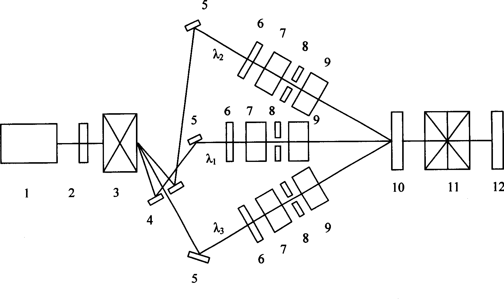
[0023] Such as figure 1 As shown, a white laser imaging interference lithography system of the present invention includes a white laser 1, an electric shutter 2, a beam splitting element 3, a perforated mirror 4, a total reflection mirror 5, an optical filter 6, and a beam expander 7. Spatial filter 8, collimating lens 9, mask 10, imaging lens 11 and resist substrate 12, these devices are arranged in turn as white laser 1, electric shutter 2, light splitting element 3, and reflector 4 with holes, The light is divided into three paths after passing through the perforated reflector 4, which are the vertical illumination optical path, the X-direction and the Y-direction biased illumination optical path, and the components of each optical path are total reflection mirror 5, filter 6, Beam expander 7, spatial filter 8, collimator lens 9, the mask 10 after the parallel light illumination output of collimator lens, the mask back is imaging lens 11, and it images mask 10 to the anti-r...


PUM


Abstract

The invention relates to an imaging interference photoengraving method and the system that adopts white laser. The feature is that is contains plural wave length of white laser light source and light splitting components, and three beams of laser with different wave length are separated from the splitting component to supply illumine on plumbing masking direction, X direction and Y direction. The system needs not any adjusting components in the exposal process. It is benefit for the application of imaging interference photoengraving technology.

Description

technical field [0001] The invention relates to an imaging interference lithography method and system using a white laser, which belongs to the improvement of the imaging interference lithography technology for producing fine patterns. Background technique [0002] Imaging interference lithography is a new lithography technology, which can realize the high resolution of interference lithography and the ability of traditional optical lithography to generate arbitrary graphics. The general imaging interference lithography method is a three-exposure method, and the general The imaging interference lithography system consists of lasers, beam expanders, filtering and collimation systems, beam splitters, masks, imaging systems and resist substrates, etc., document S.R.J.Brueck, Imaging Interferometric Lithography, Microlithography World, Winter 1998, 2 -11 and literature Xiaolan Chen and S.R.J.Brueck, Imaging Interferometric Lithography: A Wavelength Division Multiplex Approach to...

Claims


Application Information

Patent Timeline
Patent Type & Authority Applications(China)
IPC IPC(8): G03F7/20H01L21/027
Inventor 冯伯儒张锦
Owner INST OF OPTICS & ELECTRONICS - CHINESE ACAD OF SCI
Learn More