

Method for ingelligent optimizing procedure of semiconductor packing producing line
An intelligent optimization and production line technology, applied in semiconductor/solid-state device manufacturing, instruments, adaptive control, etc., can solve the problems of few simulation studies on semiconductor packaging production lines, complex and variable production systems, etc., and achieve a reasonable average occupancy rate of machines, Fast convergence speed and convenient effect
- Summary
- Abstract
- Description
- Claims
- Application Information
AI Technical Summary
Problems solved by technology
Method used
Image

Examples
Embodiment Construction
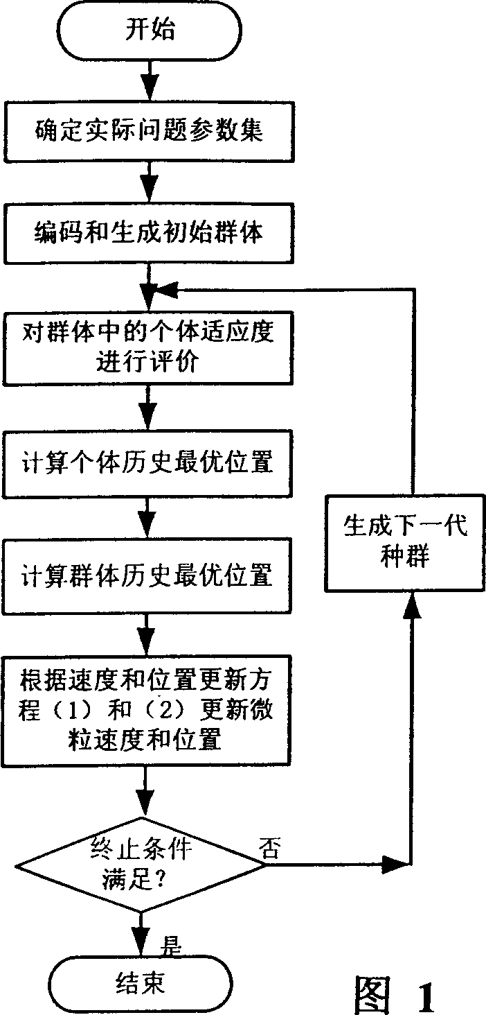
[0042] The principle of the particle swarm optimization algorithm used in the sub-problem optimization solution of the present invention is (see Figure 1):
[0043] The initial population consists of randomly generated solutions. The individuals in the population are called particles. The particles fly in the search space at a certain speed, which can be dynamically adjusted based on the flight experience of themselves and their companions. Suppose the size of the particle group is N, the particle i (i=1-N) is in D, and the coordinate position in the dimensional space can be expressed as x i =(xi1 , X i2 , K, x id , Kx iD ), the velocity of particle i is defined as the distance that the particle moves in each iteration, using v i =(v i1 , V i2 , K, v id , Kv iD ) Means. The flying speed v of the particle i in the d-th (d=1-D)-dimensional subspace id And the position update of the particles is adjusted according to the following two equations:
[0044] v id (t+1)=ωv id (t)+c 1 rand...
PUM
 Abstract
Description
Claims
Application Information