

Photovoltaic cell
A photoelectromotive force and component technology, applied in electrical components, photovoltaic power generation, circuits, etc., can solve the problems of photoelectric conversion efficiency reduction of photoelectromotive force components
- Summary
- Abstract
- Description
- Claims
- Application Information
AI Technical Summary
Problems solved by technology
Method used
Image

Examples
no. 1 approach
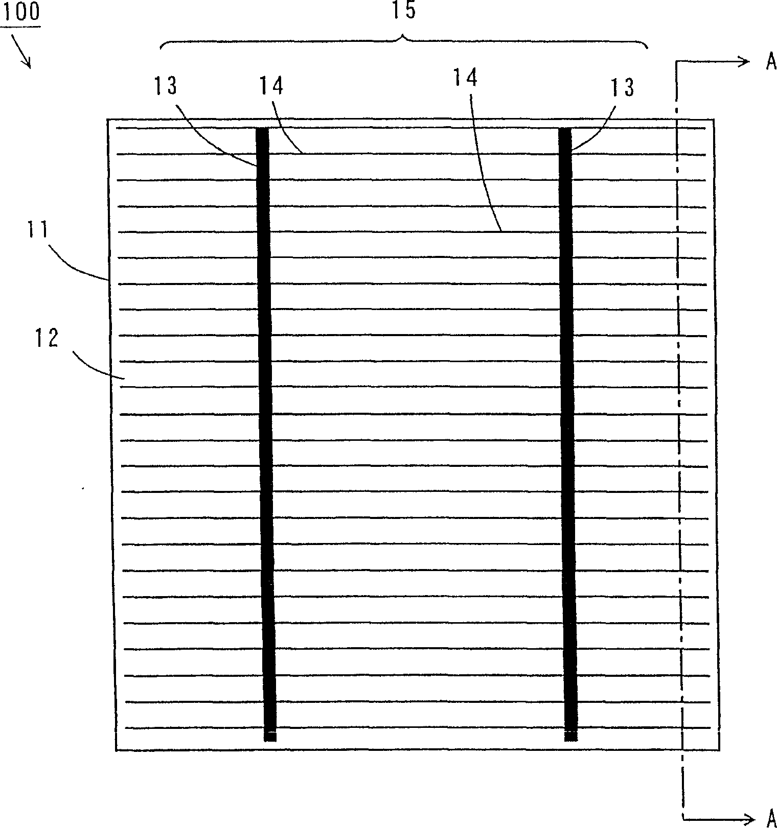
[0071] figure 1 and figure 2 It is a plan view and a bottom view of the photovoltaic element in the first embodiment of the present invention.
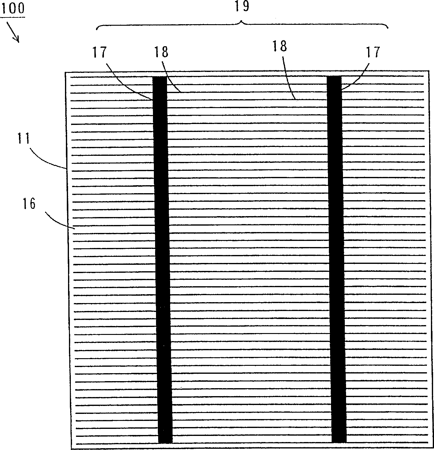
[0072] Such as figure 1 As shown, the photovoltaic element 100 includes an n-type single crystal silicon substrate 11 having a substantially square shape. On the main surface (light-receiving surface) side of the n-type single crystal silicon substrate 11, a surface electrode 12 is formed via an amorphous silicon film described later. On the surface electrode 12 , a plurality of stripe-like bus bar electrode portions 13 are formed parallel to each other, and a plurality of stripe-like finger electrode portions 14 are formed parallel to each other and perpendicular to the bus bar electrode portions 13 . The bus bar electrode portion 13 and the finger electrode portion 14 constitute a collector electrode 15 . The width of the bus bar electrode portion 13 is, for example, 1.5 mm, the width of the finger electrode portion 14 is, for ...
no. 2 approach
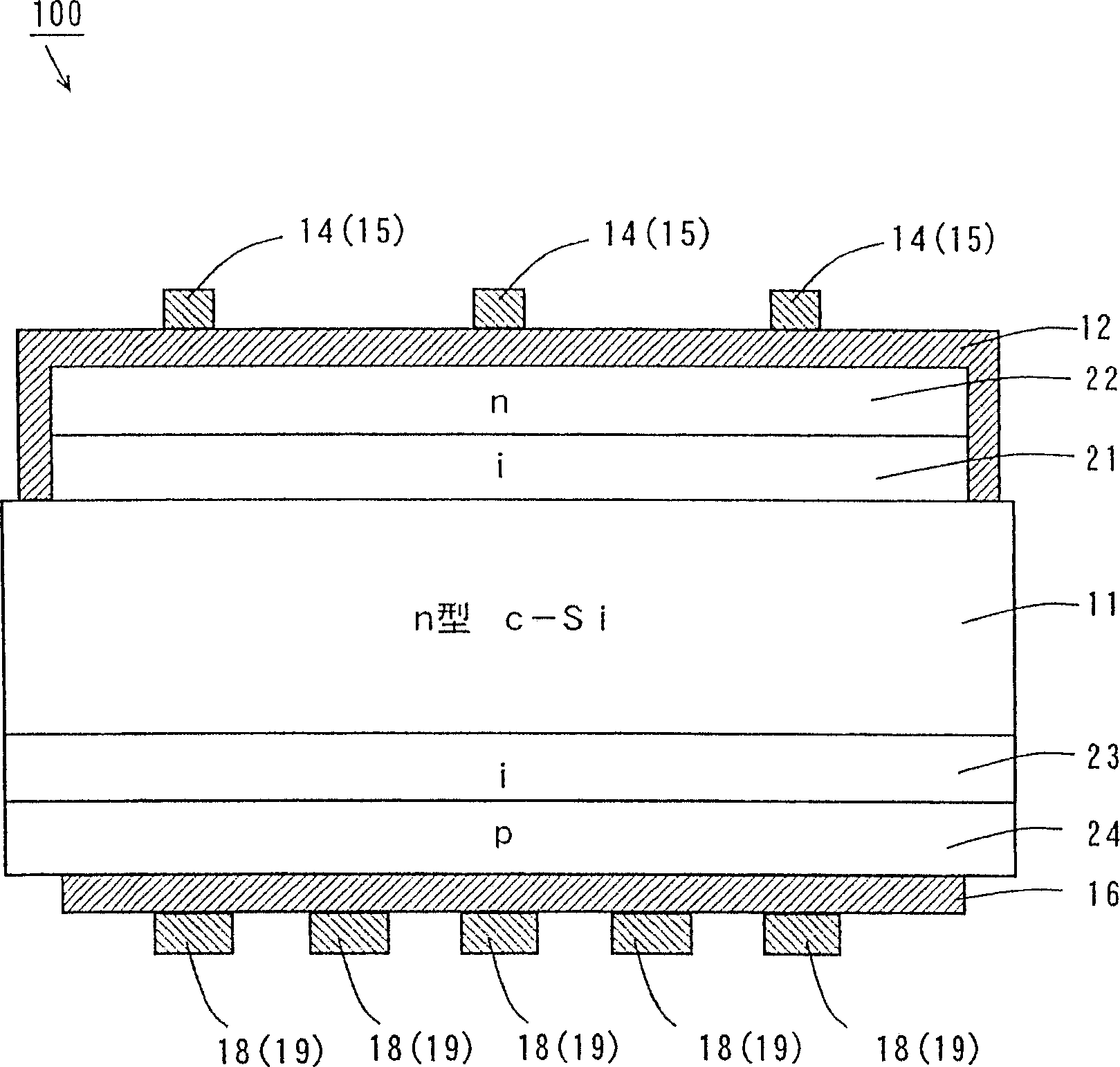
[0100] Figure 4 is a cross-sectional view showing the structure of the photovoltaic element in the second embodiment of the present invention.
[0101] Figure 4 The photoelectromotive force element 101 with image 3 The difference of the photovoltaic device 100 is as follows.
[0102] Such as Figure 4 As shown, in the photovoltaic element 101, the i-type amorphous silicon film 21a is formed on the entire area of the main surface of the n-type single crystal silicon substrate 11, and the i-type amorphous silicon film 21a except for the predetermined width of the peripheral portion is formed on the i-type amorphous silicon film 21a. area with image 3 The n-type amorphous silicon film 22 is similarly formed in the photovoltaic device 100 . Furthermore, the surface electrode 12a covering the n-type amorphous silicon film 22 is formed on the i-type amorphous silicon film 21a.
[0103] Among them, since the surface electrode 12a and image 3 The front surface electrode ...
other Embodiment approach
[0108] In the above-described embodiment, the n-type single crystal silicon substrate 11 is used as the crystal system semiconductor substrate, but it is not limited to this, and instead of the n-type single crystal silicon substrate 11, an n-type polycrystalline silicon substrate may be used, and a p-type single crystal silicon substrate may be used, A p-type polysilicon substrate can also be used.
[0109] Among them, in the case of using a p-type monocrystalline silicon substrate or a p-type polycrystalline silicon substrate, a p-type amorphous silicon film is provided instead of image 3 and Figure 4 In the n-type amorphous silicon film 22, an n-type amorphous silicon film is provided instead of the p-type amorphous silicon film 24. Thereby, the same effect as that of the above-mentioned embodiment can be acquired.
[0110] Furthermore, the i-type amorphous silicon films 21, 21a, the n-type amorphous silicon film 22, and the p-type amorphous silicon film 24 may also con...
PUM
| Property | Measurement | Unit |
|---|---|---|
| Thickness | aaaaa | aaaaa |
| Thickness | aaaaa | aaaaa |
| Thickness | aaaaa | aaaaa |
Abstract
Description
Claims
Application Information