Solid state imaging apparatus

A solid-state imaging device and pixel technology, which is applied to electric solid-state devices, radiation control devices, image communication, etc., can solve the problems of reducing the dynamic range and sensitivity S/N ratio of the imaging device, and achieves improved sensitivity, reduced pixel area, and reduced aperture. rate increase effect

Inactive Publication Date: 2006-09-27
PANASONIC CORP
View PDF3 Cites 2 Cited by
  • Summary
  • Abstract
  • Description
  • Claims
  • Application Information

AI Technical Summary

Problems solved by technology

Therefore, in the 4-transistor type CMOS sensor, the dynamic range, sensitivity, and S / N ratio of the imaging device may be lowered.

Method used


Image

  • Solid state imaging apparatus
  • Solid state imaging apparatus
  • Solid state imaging apparatus

Examples


no. 1 example

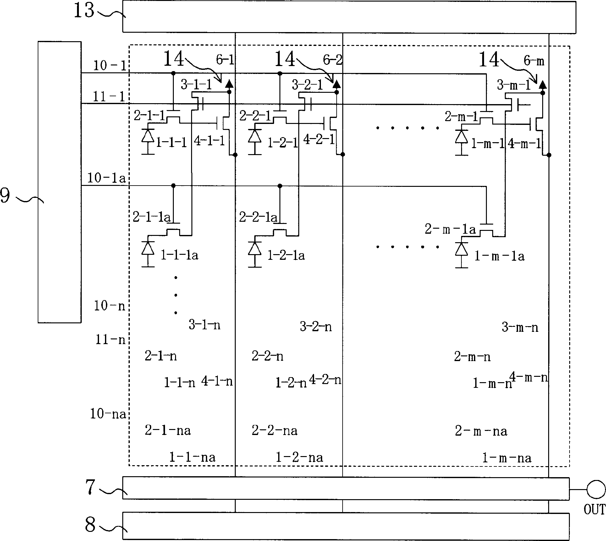
[0061] figure 1 is a diagram showing a pattern planar layout of pixel cells (pixels) of the solid-state imaging device according to the first embodiment of the present invention. In this figure, two pixels 230, 231 are shown. figure 2 is a circuit diagram showing an example of the solid-state imaging device in this embodiment.

[0062] like figure 2 As shown, the solid-state imaging device of this embodiment includes: photodiodes 1-1-1~1-m-n, transfer transistors 2-1-1~2-m-n, reset transistors 3-1-1~3-m-n, Amplifying transistors 4-1-1 to 4-m-n, row signal lines 6-1 to 6-m, row signal accumulation section 7, column selection section 8, row selection section 9, transfer transistor control lines 10-1 to 10- n. Reset transistor control lines 11 - 1 to 11 - n , load transistor group 13 and pixel portion power supply 14 . Here, both m and n are integers greater than or equal to 2.

[0063] The photodiodes 1-1-1~1-m-n convert the incoming light into electrical signals; the tr...

no. 1 example 1

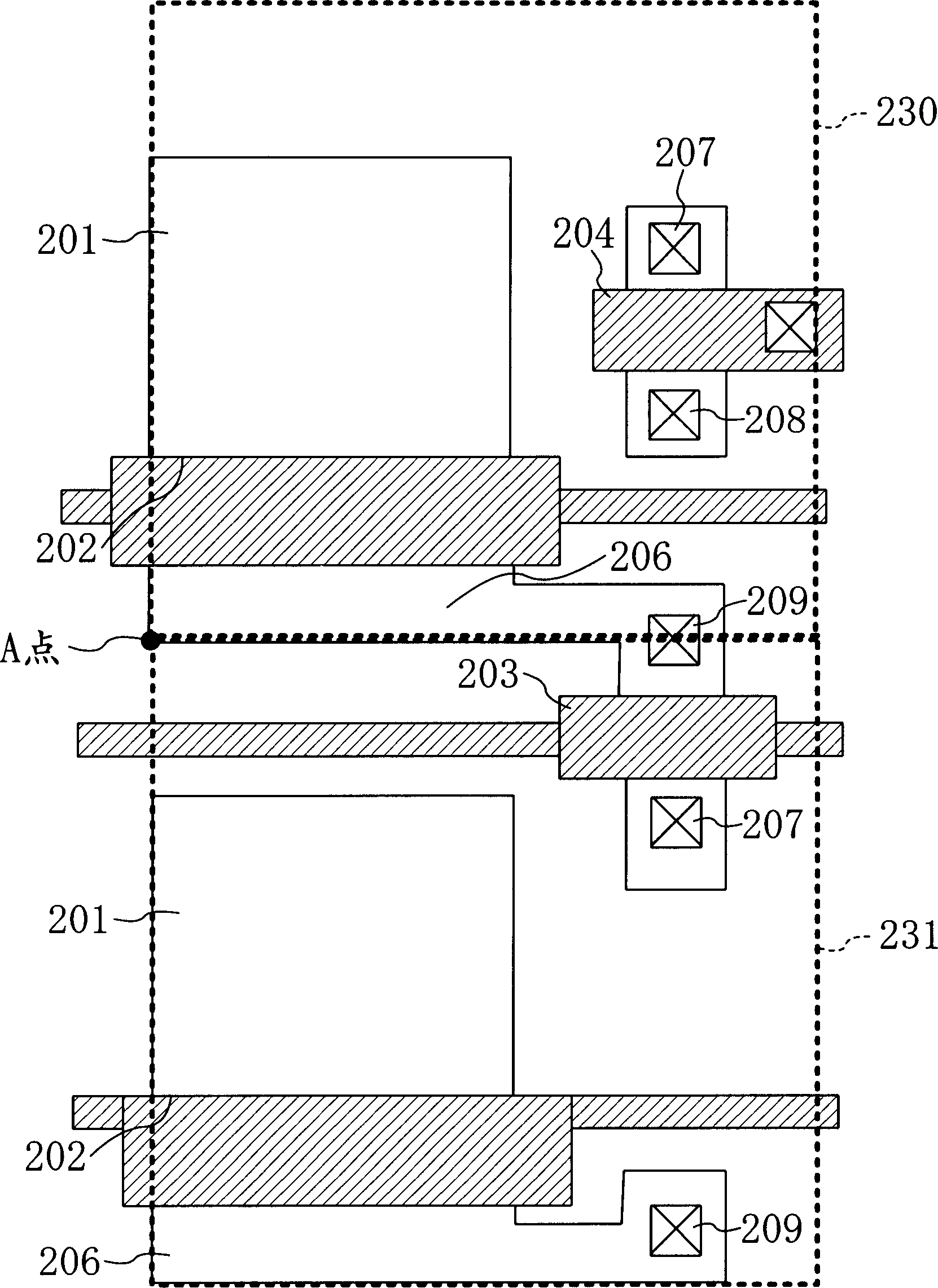
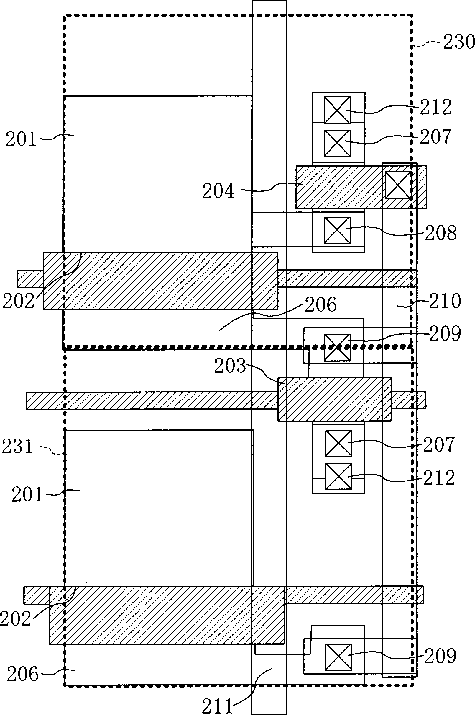
[0083] Figure 5 It is a diagram showing the pattern plan layout of the pixel cell portion of the solid-state imaging device according to the second embodiment of the present invention. This figure shows specific two pixel cell portions in a plurality of pixel cells of the same shape that are periodically arranged in a solid-state imaging device. Like the first embodiment, the pattern plan layout of the pixel cell in this embodiment is the pattern plan layout of a three-transistor type CMOS sensor in which two pixels share a reset transistor and an amplification transistor. Just to add, Figure 5 Aluminum wiring and the like are not shown, and the circuit configuration of the pixel cell as the solid-state imaging device of this embodiment is described in Figure 13 In the same pixel circuit as a plurality of pixels share 1 amplification device.

[0084] The adjacently arranged first pixel 230 and the second pixel 231 each have: a photodiode 201; a transfer transistor for tr...


PUM


Abstract

A 3TrCMOS solid-state image pickup device is provided with a plurality of pixels, including a first pixel (230) and a second pixel (231) adjacent to each other. Each of the adjacent pixels is provided with a photodiode (201) for converting light into a signal charge and a transmission transistor for reading out the signal charge generated by the photodiode (201). The first pixel (230) is provided with a reset transistor whose one end is connected with the both photodiodes (201) in the first pixel (230) and in the second pixel (231) and the other end is supplied with a power supply voltage. The second pixel (231) is provided with a gate electrode (204) connected with the both transmission transistors in the fist pixel (230) and the second pixel (231), and an amplifying transistor whose drain is supplied with a power supply voltage.

Description

technical field [0001] The present invention relates to a solid-state imaging device provided with pixels having MOS transistors, and more particularly to a solid-state imaging device having a pattern layout in a pixel cell and its layout. Background technique [0002] Solid-state imaging devices are classified into FET type and CCD type having a MOS structure composed of metals, oxides, and semiconductors, depending on how carriers move by photoelectric conversion. This solid-state imaging device is used in solar cells, cameras, copiers, facsimile machines, and the like, and technological improvements are being made to improve the light conversion efficiency and the integration density of the device. One of the amplifying solid-state imaging devices that includes an amplifying element in a pixel, there is a CMOS process compatible sensor (hereinafter abbreviated as a CMOS sensor). This type of sensor is described in Non-Patent Document 1 and the like. [0003] Fig. 7(a) i...

Claims


Application Information

Patent Timeline
Patent Type & Authority Applications(China)
IPC IPC(8): H01L27/146H04N5/335H04N5/361H04N5/369H04N5/374
CPCH01L27/14603H01L27/14609H04N5/37457H01L27/14641H04N25/778H04N25/76
Inventor 太田宗吾内田干也
Owner PANASONIC CORP
Why Eureka
Try Eureka