

Semiconductor interconnect structure and NOR type quickflashing memory and method of manufacture
A manufacturing method and interconnection technology, which are applied in semiconductor/solid-state device manufacturing, semiconductor devices, semiconductor/solid-state device components, etc., can solve the problem that the area of NOR-type flash memory cannot be further reduced, and increase NOR-type flash memory Body size and other issues, to achieve the effect of reducing the memory area, reducing the memory area, and reducing the memory area
- Summary
- Abstract
- Description
- Claims
- Application Information
AI Technical Summary
Problems solved by technology
Method used
Image

Examples
no. 1 example
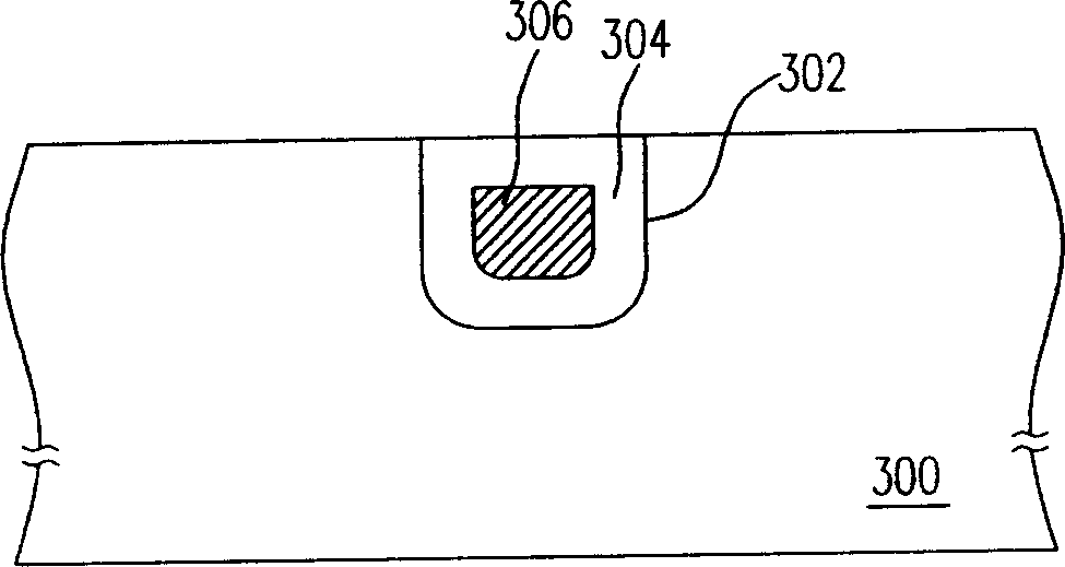
[0054] see image 3 Shown is a schematic cross-sectional view of a semiconductor interconnection according to the first embodiment of the present invention. see image 3 , the semiconductor interconnection includes a substrate 300 , an insulating layer 304 and a conductive layer 306 . Wherein, a trench 302 has been formed in the substrate 300, and an insulating layer 304 is disposed in the trench 302, and its material is, for example, silicon oxide. Furthermore, the conductive layer 306 is disposed in the insulating layer 304 and covered by the insulating layer 304 , and its material is, for example, doped polysilicon.
[0055] Due to the semiconductor interconnection in the first embodiment, the conductive layer 306 is disposed in the insulating layer 304, which can effectively save space and reduce the size of the semiconductor device.
no. 2 example
[0057] see Figure 4A ~ Figure 4C Shown is a cross-sectional view of the manufacturing process of a semiconductor interconnection line according to the second embodiment of the present invention. First, see Figure 4A Firstly, a substrate 400 is provided, and a trench 406 has been formed in the substrate 400. The formation method is, for example, firstly forming a patterned mask layer 404 on the substrate 400, and then performing an etching process to form it. Wherein, the material of the patterned mask layer 404 is, for example, silicon nitride. In addition, before forming the patterned mask layer 404 , the pad oxide layer 402 may be formed on the substrate 400 to increase the adhesion of the patterned mask layer 404 . The material of the pad oxide layer 402 is, for example, silicon oxide, and the forming method is, for example, thermal oxidation.
[0058] Next, see Figure 4B A liner oxide layer 408 is formed on the surface of the trench 406, and its material is, for exa...
no. 3 example
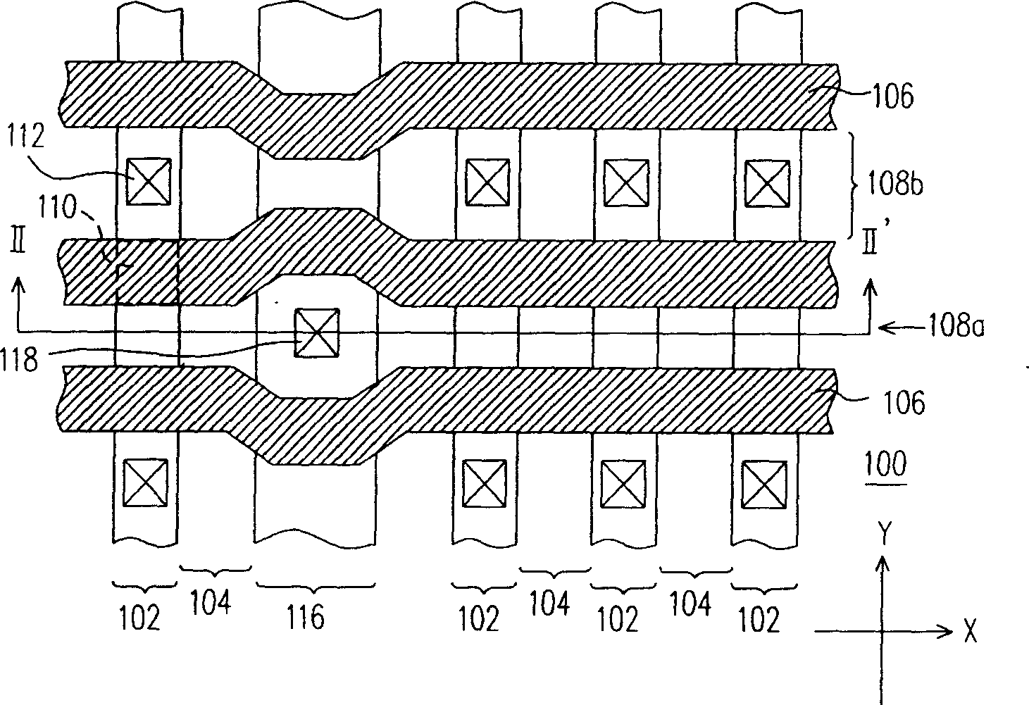
[0063] see Figure 5A Shown is a top view of a NOR flash memory according to the third embodiment of the present invention, Figure 5B yes Figure 5A The schematic cross-sectional view of the B-B' line of , and Figure 5C yes Figure 5A The schematic cross-section of the line C-C'.
[0064] Please also see Figure 5A to Figure 5C The NOR flash memory provided in this embodiment includes a substrate 500, several control gates 502, several trenches 504, several source regions 506, several drain regions 508, several isolation structures 510, A plurality of conductive blocks 514 , a plurality of floating gates 516 , a plurality of tunnel oxide layers 518 and a dielectric layer 520 .
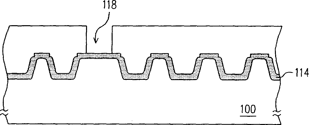
[0065] Wherein, the control gates 502 are arranged on the substrate 500 along the X direction, and the trenches 504 are arranged on the surface of the substrate 500 along the Y direction. Moreover, the source region 506 is located in the substrate 500 and the trench 504 on one side of the contr...
PUM
 Abstract
Description
Claims
Application Information