Semiconductor device and method of manufacturing the same
A technology of semiconductors and conductive components, which is applied in the direction of semiconductor devices, semiconductor/solid-state device parts, electric solid-state devices, etc., which can solve problems such as deterioration of high-frequency characteristics, deterioration of high-frequency characteristics of the semiconductor device 105, large parasitic inductance, etc., and achieve reduction Effects of parasitic inductance, improvement of high-frequency characteristics, and improvement of yield
- Summary
- Abstract
- Description
- Claims
- Application Information
AI Technical Summary
Problems solved by technology
Method used
Image

Examples
no. 1 approach
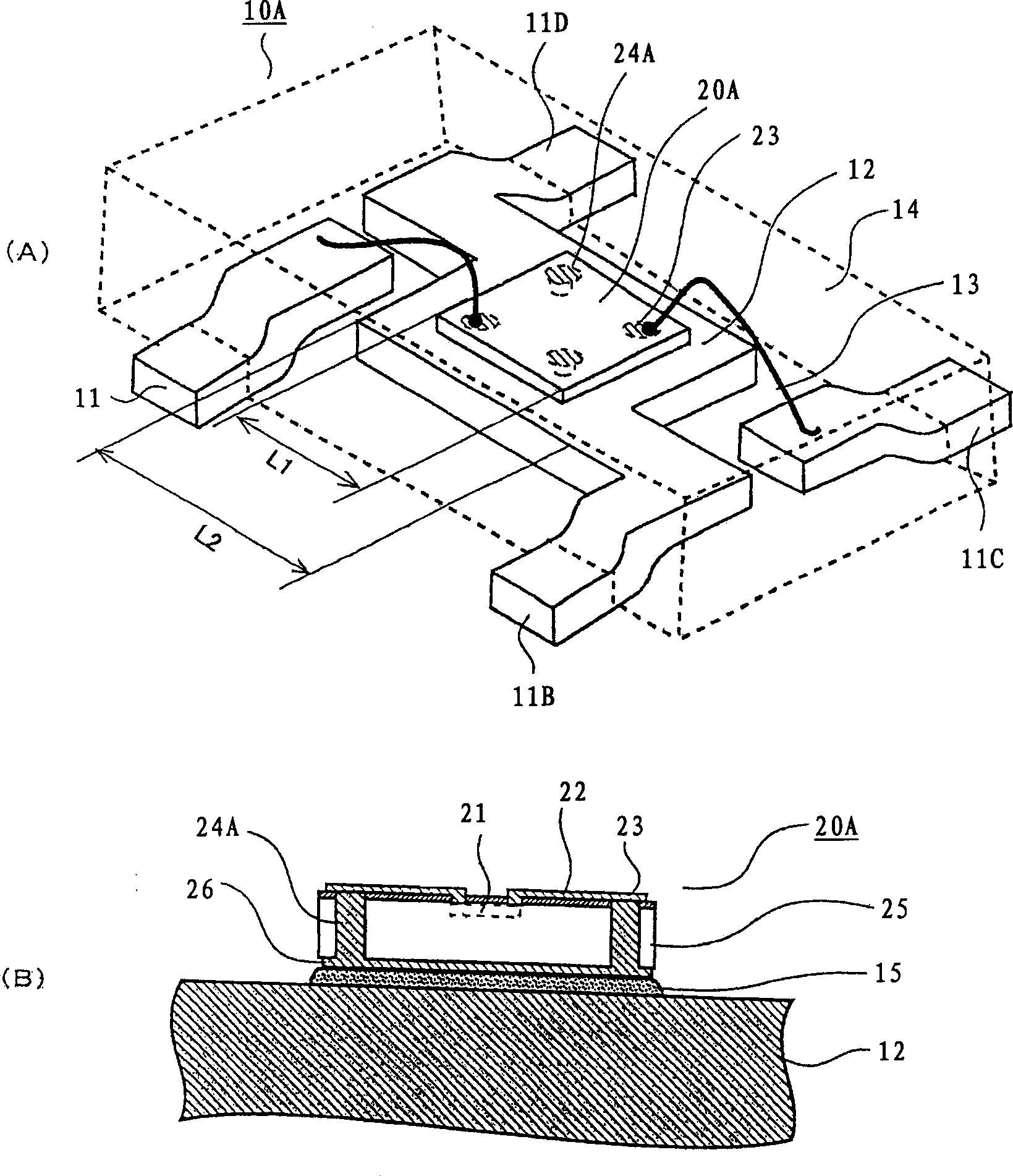
[0072] In this method, refer to Figure 1 to Figure 5 A structure of a semiconductor device having a through-electrode penetrating a semiconductor substrate will be described.
[0073] refer to figure 1 The configuration of a circuit device 10A including a semiconductor device 20A of the present invention will be described. figure 1 (A) is a perspective view of the circuit device 10A, figure 1 (B) is a cross-sectional view of the semiconductor device 20A.
[0074] refer to figure 1 (A) Here, the semiconductor device 20A is provided in the lead frame type circuit device 10A. Specifically, the semiconductor device 20A is fixed on the upper surface of the land 12 arranged in the center. In addition, the two lead wires 11D and 11B are extended to the outside from the end of the land 12 . In addition, a lead wire 11A and a lead wire 11C are provided close to the land surface 12 . The land 12, the lead wire 11A, etc. are an example of a conductive member. As a conductive...
no. 2 approach
[0116] Second, refer to Figure 6 ~ Figure 8 illustrate Figure 4 (A) The manufacturing method of the semiconductor device 20A of the structure shown. First, refer to Image 6 A method of forming the active region 21 composed of bipolar transistors will be described.
[0117] refer to Image 6 (A), first, on the surface of the P-type semiconductor substrate 42 with a thickness of about 600 μm, N + type buried layer 43 . Further, N is formed on the P-type semiconductor substrate 42 - Type epitaxial layer 31. N - The thickness of the epitaxial layer 31 is about 1.5 μm. Then, by oxidizing the entire face, the N - An oxide film 32 with a thickness of about 0.05 μm is formed on the epitaxial layer 31 .
[0118] refer to Image 6 (B) Next, a groove 33 is formed surrounding an active region to be formed, and the inside of the groove 33 is filled with an oxide film. Here, the oxide film 32 and the N - Type epitaxial layer 31. Oxide film 32 is removed using CF 4 gas-like...
no. 3 approach
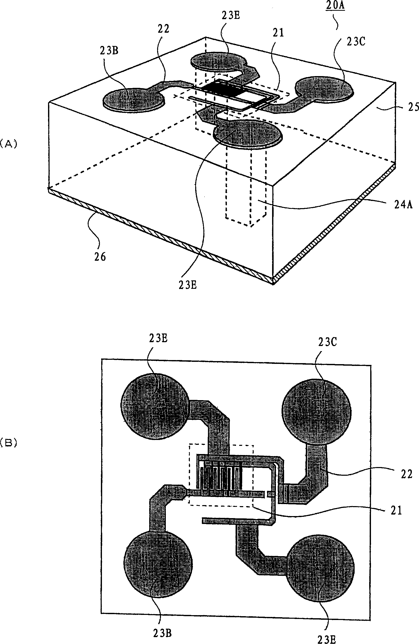
[0136] In this embodiment, refer to Figure 9 illustrate Figure 4 (C) The manufacturing method of the semiconductor device 20B of the structure shown. The manufacturing method of this embodiment is basically the same as that of the above-mentioned second embodiment, except that the side wall insulating film is not formed on the inner wall of the through-hole 24B.
[0137] Specifically, refer to Figure 9 (A), first, the active region 21 composed of, for example, a bipolar transistor is formed. Furthermore, the active region 21 is separated from the elements by forming the groove 33 surrounding the active region 21 . In addition to the groove 33, the isolation of the active region 21 may also be performed using a PN junction isolation and a LOCOS oxide film. In addition, electrodes connected to the respective regions constituting the active region 21 are formed on the surface of the oxide film 32 . Here, the emitter pad electrode 23E and the collector pad electrode 23C ar...
PUM
| Property | Measurement | Unit |
|---|---|---|
| Diameter | aaaaa | aaaaa |
| Thickness | aaaaa | aaaaa |
| Thickness | aaaaa | aaaaa |
Abstract
Description
Claims
Application Information
 - Generate Ideas
- Intellectual Property
- Life Sciences
- Materials
- Tech Scout
- Unparalleled Data Quality
- Higher Quality Content
- 60% Fewer Hallucinations
Browse by: Latest US Patents, China's latest patents, Technical Efficacy Thesaurus, Application Domain, Technology Topic, Popular Technical Reports.
© 2025 PatSnap. All rights reserved.Legal|Privacy policy|Modern Slavery Act Transparency Statement|Sitemap|About US| Contact US: help@patsnap.com