Method for reducing critical dimension

A key size, photomask technology, applied in photomechanical processing of originals, patterned surface photoengraving process, instruments, etc. The effect of size

Inactive Publication Date: 2006-11-22
UNITED MICROELECTRONICS CORP
View PDF0 Cites 7 Cited by
  • Summary
  • Abstract
  • Description
  • Claims
  • Application Information

AI Technical Summary

Problems solved by technology

However, the plasma trimming process is not ideal for trimming the end of the wire due to the characteristics of the process itself, and cannot maintain the predetermined wire length
In addition, in order to avoid that the photoresist may be completely removed, this process also has a shrink volume limit
In addition, the plasma trim process takes a long time, which reduces the efficiency of the photolithography process
Moreover, due to the ion bombardment, the properties of the exposed part of the photoresist layer will be changed, and the rework process (rework process) cannot be carried out. It may be necessary to spend more time to redeposit the photoresist layer to improve the manufacturing process. cost

Method used


Image

  • Method for reducing critical dimension
  • Method for reducing critical dimension
  • Method for reducing critical dimension

Examples


Embodiment Construction

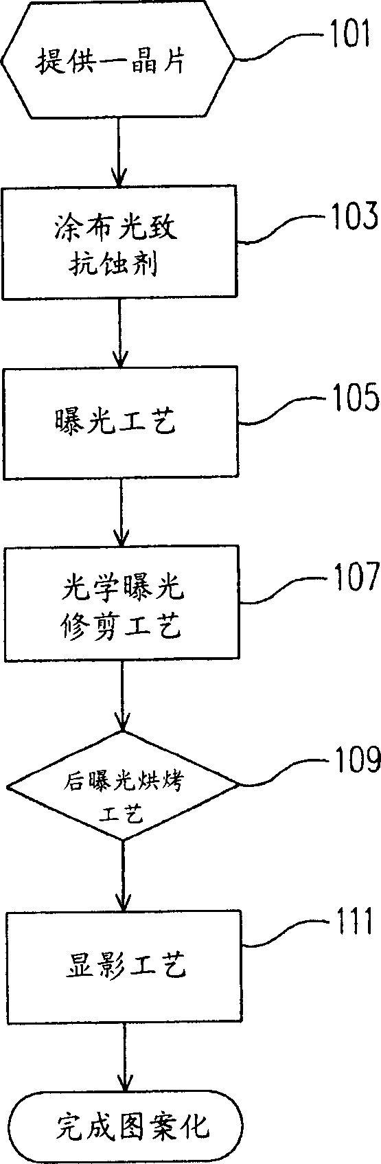
[0030] figure 1 Illustrated is a step-by-step diagram of the manufacturing process of the method for reducing critical dimensions according to a preferred embodiment of the present invention. Figure 2A to Figure 2D Illustrated is a cross-sectional view of the manufacturing process of a method for reducing critical dimensions according to a preferred embodiment of the present invention.

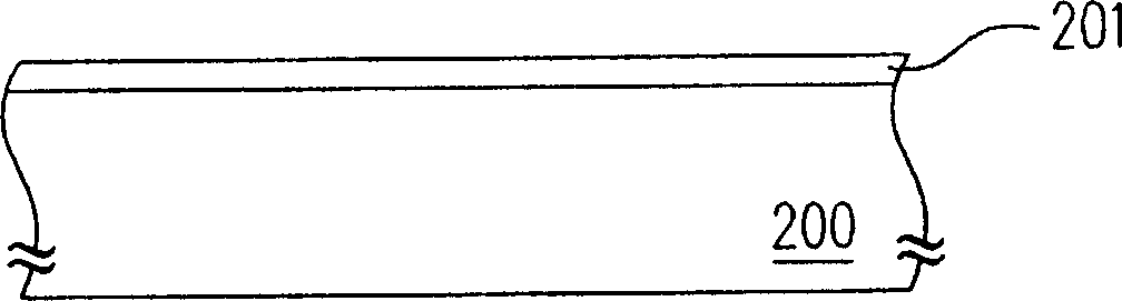
[0031] Please refer to figure 1 as well as Figure 2A , first provide a wafer 200 (step 101). The wafer 200 may be a wafer 200 on which transistors, memory cells, or other semiconductor elements have been formed, or a wafer 200 on which no semiconductor elements have been formed. The surface of the wafer 200 may be a dielectric layer, a conductive layer, a protective layer or any film layer requiring etching, doping and other processes. Next, a photoresist layer 201 is coated on the wafer 200 (step 103). The coating method is, for example, spin coating (spin coating), and the material of ...


PUM

PropertyMeasurementUnit
sizeaaaaaaaaaa

Abstract

A method for reducing critical dimension is provided. An exposure process and a develop process are performed on a photoresist layer. An optical trim exposure process is performed between the exposure process and the development process or before the exposure process. The optical trim expsoure process is performed to expose the photoresit layer by using a fully open mask of which the transmission rate is greater than zero. Because of the performance of the optical trim exposure process, the critical dimension of the photoresist layer can be reduced without substantially changing the characteristics of the photoresist layer.

Description

technical field [0001] The present invention relates to a semiconductor manufacturing method, in particular to a method for reducing critical dimension (CD). Background technique [0002] Today, with the vigorous development of integrated circuits, the requirements for component integration are getting higher and higher, and the size design of the entire circuit component must be reduced accordingly. And the key lies in the technology of photolithography (photolithography) process. [0003] However, due to the limitation of the yellow photolithography process, it is impossible to directly obtain a smaller critical dimension by improving the photolithography process. Therefore, a process for trimming the photoresist has been developed in the industry, including a chemical trim process and a plasma trim process, which are described as follows. [0004] The chemical trimming process is to immerse the patterned photoresist layer and the entire underlying wafer in an environmen...

Claims


Application Information

Patent Timeline
Patent Type & Authority Applications(China)
IPC IPC(8): G03F7/20G03F1/00H01L21/027
CPCG03F7/2022G03F7/38
Inventor 张圣岳吴得鸿黄国俊
Owner UNITED MICROELECTRONICS CORP
Why Eureka
Try Eureka