Bonding wire and integrated circuit device using the same

A technology for bonding lead wires and coating layers, which is applied in the direction of circuits, electrical components, and electrical solid devices, and can solve problems such as poor drawability, difficult drawing of high melting point metals, and short mold life

Inactive Publication Date: 2006-11-22
SUMITOMO ELECTRIC IND LTD
View PDF3 Cites 7 Cited by
  • Summary
  • Abstract
  • Description
  • Claims
  • Application Information

AI Technical Summary

Problems solved by technology

[0019] However, high-melting point metals are generally difficult to draw, and it has been pointed out that the methods with the above-mentioned excellent characteristics still have the following 1-4 problems, which all need to be improved
[0020] 1. Higher frequency of lead breakage and lower yield compared to gold
[0021] 2. The drawing die is easy to wear, and the life of the die is short
[0022] 3. Although the possibility of delamination of the coating layer is reduced, there is stil

Method used


Image

  • Bonding wire and integrated circuit device using the same
  • Bonding wire and integrated circuit device using the same
  • Bonding wire and integrated circuit device using the same

Examples


example 1

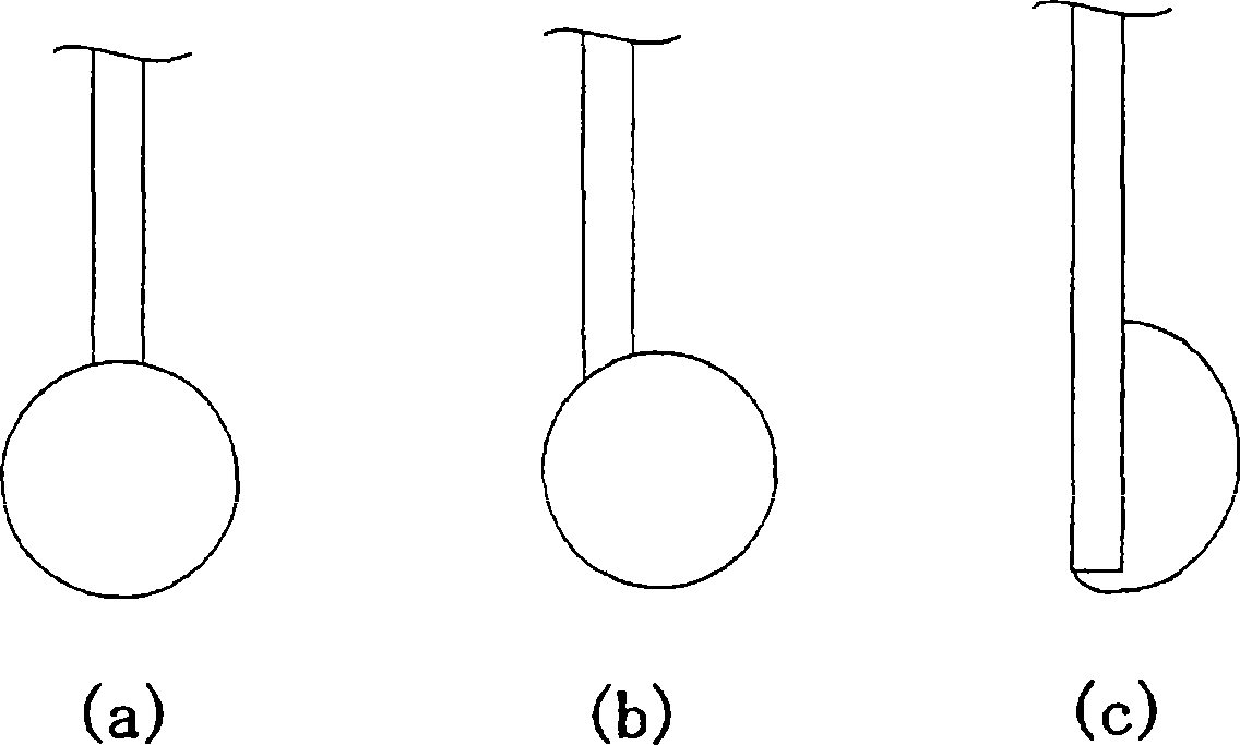
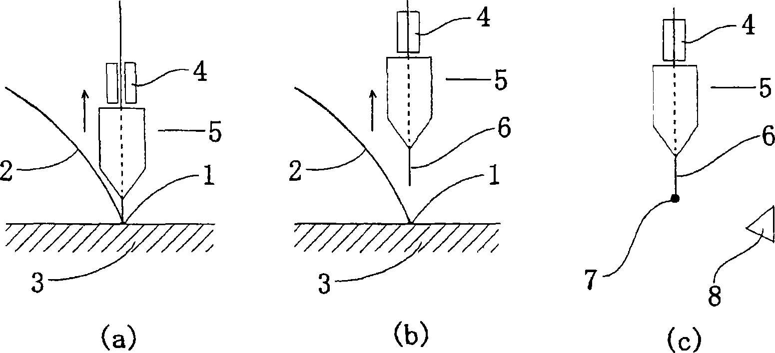
[0104] A 0.8 μm-thick coating layer was formed by electroplating on a core copper lead having a purity of 99.995% and a diameter of 200 μm. By drawing and annealing the wire, various types of bonding wires having a core diameter of 25.2 μm and a coating layer thickness of 0.1 μm were produced. Using various leads, 100 balls with a diameter of 60 μm were formed by using a bonding machine (model FB 137 manufactured by Kaijo Co., Ltd.), and the number of occurrences of shape defects in which the center of the ball was displaced from the center of the lead was checked. The results are shown in Table 1 together with the core and coating materials used.

[0105] The wet contact angle when the core material was melted was measured by using high temperature wettability test apparatus WET1200 manufactured by ULVAC-RIKO in the following manner.

[0106] A piece of material produced by compressing 2.5 mm sized balls of core material into an easily mountable shape was placed on a piece of ...

example 2

[0110] (1) An approximately 0.04 μm thick gold underplating film was formed by underplating on a copper lead having a purity of 99.995% and a diameter of 200 μm. After that, a 0.8 µm thick palladium plating film was formed. Copper bonding wires are produced by drawing and annealing the wires. Various bonding wires have a copper core diameter of 25.2 μm, a palladium layer (coating layer) thickness of 0.1 μm, and a gold layer (different metal layer) thickness of about 0.005 μm, the elongation is 15%. Samples with various radii of curvature were produced by adjusting the diameter of the guide roll and the tension used to wind the lead wire around the spool. Using various samples, a 208-pin QFP (copper lead frame, silver spot plating) with a loop length of about 4 mm was applied using a bonding machine (model EAGLE AB339 manufactured by ASM) by applying a load of 80 g and an ultrasonic energy of 160 Bonding is performed on the board and the defect rate is checked (ppm: the numbe...

example 3

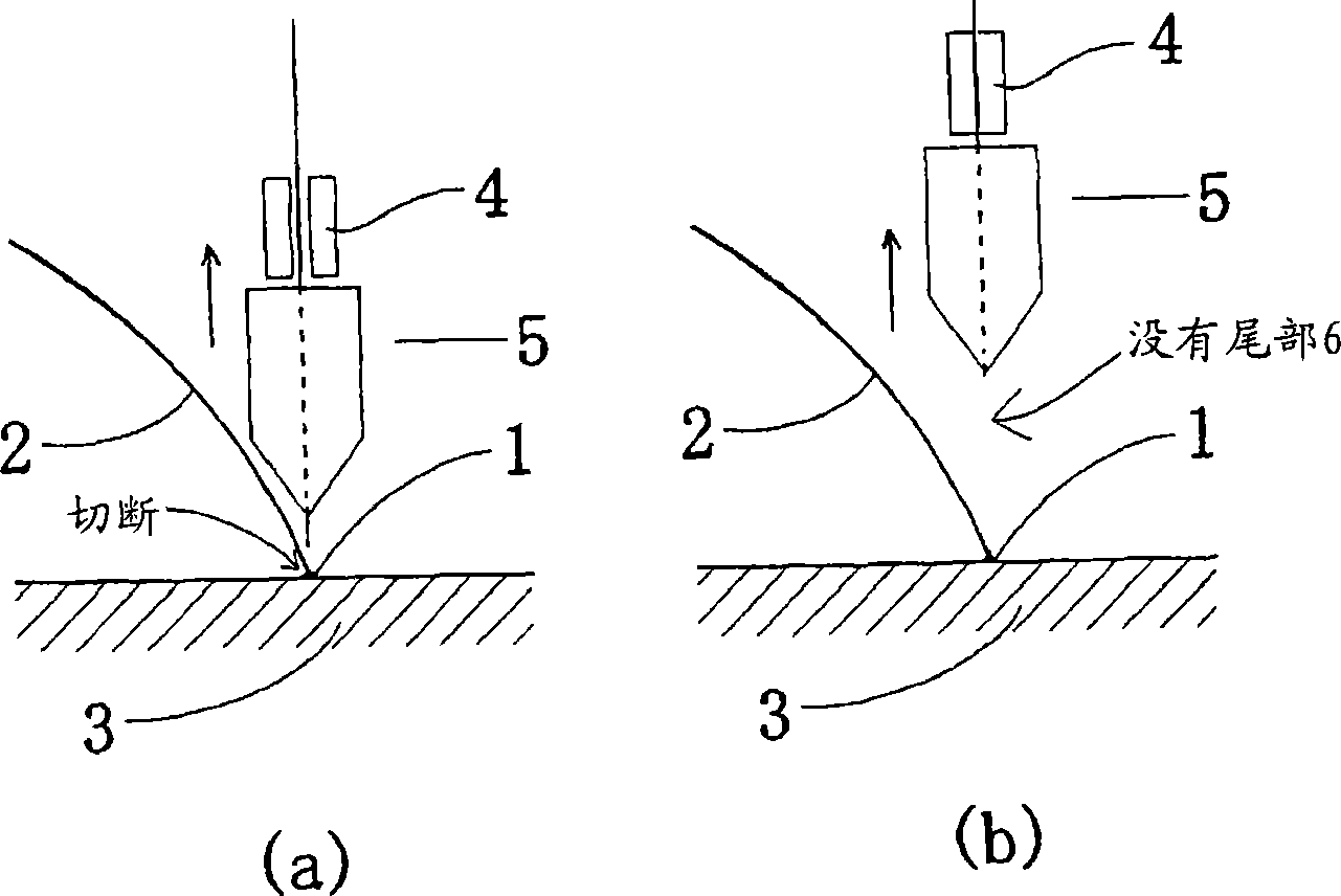
[0115] A gold underplating film with a thickness of about 0.04 μm was formed by underplating on a copper lead having a purity of 99.995% and a diameter of 200 μm. After that, a 0.8 µm thick palladium plating film was formed. Copper bonding wires with various yield strength values ​​were produced by drawing and annealing the wires. The copper core diameter of various bonding wires was 25.2 μm, the thickness of the palladium layer (coating layer) was 0.1 μm, and the gold layer (different metals) layer) has a thickness of about 0.005 μm. Various copper bonding leads have a radius of curvature of 40mm. Bonding was performed on a 208-pin QFP (copper leadframe, silver plating) with a loop length of approximately 4 mm using a bonding machine (model EAGLE AB339 manufactured by ASM) by applying a load of 80 g and varying ultrasonic energy and inspecting using various leads. The defect rate (ppm: the number of short-tail defects and no-stem defects occurring per million bonds) is belo...


PUM

PropertyMeasurementUnit
Melting pointaaaaaaaaaa
Diameteraaaaaaaaaa
Thicknessaaaaaaaaaa

Abstract

A bonding wire which has a core material and formed on the core material, a coating layer comprising a metal having a melting point higher than that of the core material and further has at least one of the following characteristics: 1. the wet contact angle of the molten core material with the coating material is 20 degree or more, 2. the curvature radius of a circular arc, which is formed when the bonding wire is allowed to hang down so that the tip thereof contacts with a horizontal plane and the wire is cut at the point being upper from the tip by 15 cm and the cut wire is allowed to fall on the horizontal plane, is 35 mm or more. 3. 0.2 % offset yield strength is 0.115 to 0.165 mN/mum<2>, and 4. the coating layer has a Vickers hardness of 300 or less.

Description

technical field [0001] The present invention relates to a bonding lead for connecting electrodes on an integrated circuit device (IC, LSI, transistor, etc.) to wires on a circuit wiring substrate (lead frame, ceramic substrate, printed circuit board, etc.) , and also relates to an integrated circuit device using such a bonding wire. Background technique [0002] A ball bonding method using bonding wires is used as a method of connecting an integrated circuit device to a circuit wiring board. [0003] The ball bonding method is a common implementation process in which one end of the bonding wire guided by a movable capillary (hereinafter referred to as "bonding tool") is melted by an electrical discharge between it and an electrode torch to A ball is formed at that end, after which the ball is pressed against the first bonding point to form a ball bond on it, then, as the lead is fed out, the bonding tool moves to the second bonding point in the same manner (but this time d...

Claims


Application Information

Patent Timeline
IPC IPC(8): H01L21/60
CPCH01L24/43H01L2224/43H01L2224/4312H01L2224/4321H01L2224/43825H01L2224/43827H01L2224/43848H01L2224/45H01L2224/45015H01L2224/45139H01L2224/45144H01L2224/45147H01L2224/45565H01L2224/45572H01L2224/456H01L2224/45644H01L2224/45655H01L2224/45664H01L2224/45669H01L2224/45673H01L2224/4845H01L2924/00011H01L2924/01004H01L2924/01005H01L2924/01006H01L2924/01007H01L2924/01012H01L2924/01013H01L2924/01016H01L2924/01022H01L2924/01024H01L2924/01025H01L2924/01027H01L2924/01028H01L2924/01029H01L2924/0103H01L2924/01033H01L2924/0104H01L2924/01044H01L2924/01045H01L2924/01046H01L2924/01047H01L2924/0105H01L2924/01075H01L2924/01076H01L2924/01077H01L2924/01078H01L2924/01079H01L2924/01082H01L2924/01088H01L2924/01204H01L2924/14H01L2924/15747H01L2924/19043H01L2924/20751H01L2924/20752H01L2924/20753H01L2924/01008H01L2924/01026H01L2924/01001H01L2924/00014H01L2924/013H01L2924/00H01L2924/2076H01L2924/01015H01L2924/01049H01L2924/00012
Inventor 改森信吾野中毅井冈正则
Owner SUMITOMO ELECTRIC IND LTD
Why Eureka
Try Eureka