Structure of semiconductor metal capacitor and etching method

A metal capacitor and semiconductor technology, which is applied to the etching of semiconductor metal capacitors and the structure of semiconductor metal capacitors, can solve the problems of inability to achieve large-capacity capacitors, large dielectric coefficient of nitride films, and many pinholes in nitride films. Achieve the effect of simple and easy etching method, large dielectric coefficient and uniform thickness

Inactive Publication Date: 2007-01-10
SHANGHAI HUA HONG NEC ELECTRONICS
View PDF0 Cites 4 Cited by
  • Summary
  • Abstract
  • Description
  • Claims
  • Application Information

AI Technical Summary

Problems solved by technology

The oxide film has good film quality and less pinholes, but the dielectric coefficient is small, only about 4, which cannot achieve large-capacity capacitance; the nitride film has a large dielectric coefficient, which can reach 7.8, and is more commonly used
However, there are many pinholes in the nitride film, which is easy to cause leakage

Method used


Image

  • Structure of semiconductor metal capacitor and etching method
  • Structure of semiconductor metal capacitor and etching method
  • Structure of semiconductor metal capacitor and etching method

Examples


Embodiment Construction

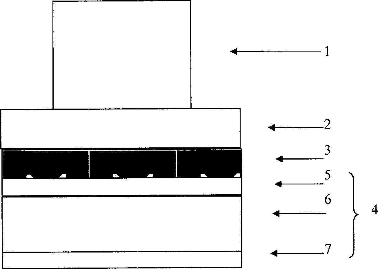
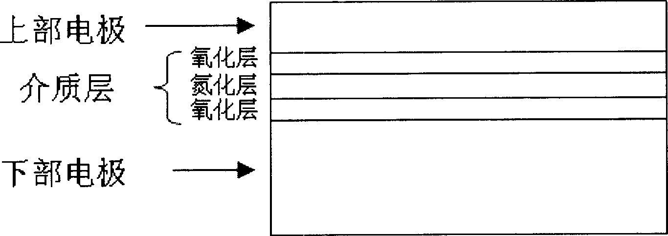
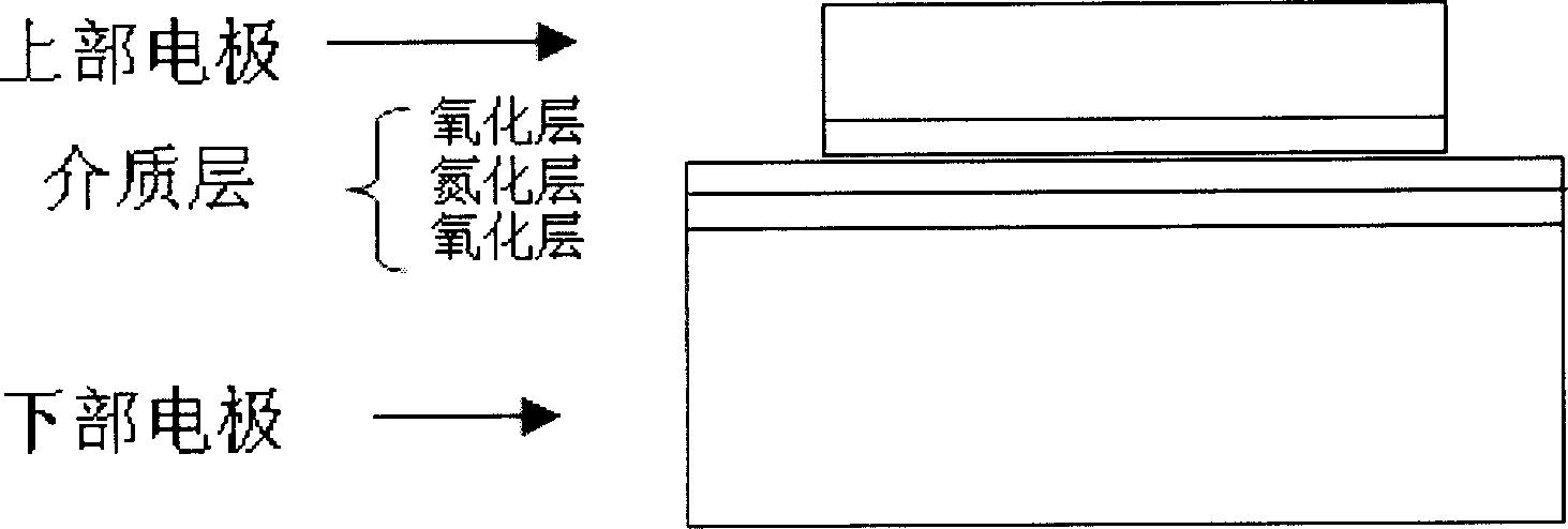
[0013] Such as figure 2 Therefore, a semiconductor metal capacitor of the present invention includes a lower electrode, a dielectric layer and an upper electrode from bottom to top, and the dielectric layer includes an oxide film layer, a nitride film layer and another oxide film layer from bottom to top. film layer. The capacitor structure uses a composite layer composed of oxide film and nitride film as the dielectric layer, so that the semiconductor metal capacitor not only retains the advantages of good oxide film quality, less pinholes, and large dielectric coefficient of the nitride film, but also overcomes the advantages of the oxide film. Small dielectric coefficient and many pinholes in the nitride film can easily cause leakage.

[0014] The present invention also includes an etching method for realizing the above-mentioned semiconductor metal capacitor structure, the steps of which include firstly etching off the upper electrode, and then using the condition of an ...


PUM


Abstract

The structure of semiconductor alloy capacitance includes lower electrode, dielectric layer and upper electrode in sequence from lower to upper. The dielectric layer includes an oxide film layer, an ammoniated film layer, and another oxide film layer from lower to upper. Using multiple dielectric layers, the structure makes semiconductor alloy capacitance possible to reserve each advantage of oxide film layer, and ammoniated film layer, and overcome disadvantage of small dielectric coefficients of the film layers, and lot of pinholes on the film layers. The invention also discloses method for etching the capacitance. After etching out upper electrode, and using condition of selection ration in high etching speed, the method etches out uppermost oxide film layer, and stops etching operation when the ammoniated film layer is met. Advantages are: easy of implementation, large technical window for etching time, even thickness of dielectric layer, and raised quality and efficiency.

Description

technical field [0001] The invention relates to a structure of a capacitor, in particular to a structure of a semiconductor metal capacitor; the invention also relates to an etching method of a semiconductor metal capacitor. Background technique [0002] In the process of semiconductor manufacturing, it is often necessary to grow a dielectric layer and a titanium nitride metal film on the metal aluminum line to form a metal capacitor. Metal capacitors require specific etching procedures to give them the desired shape. The structure of metal capacitors before etching can be found in figure 1 . The lowermost layer is a metal layer 7 of titanium / titanium nitride, above which there is a metal layer 6 of metal aluminum, and a layer of metal layer 5 of titanium / titanium nitride is further formed on the top of the metal aluminum layer 6. The above three layers 5, 6 , 7 jointly form the lower electrode 4 of the metal capacitor. On the lower electrode 4 is a dielectric layer 3 as...

Claims


Application Information

Patent Timeline
Patent Type & Authority Applications(China)
IPC IPC(8): H01L29/92H01L27/108H01L21/00H01L21/02H01L21/329H01L21/8242
Inventor 吕煜坤
Owner SHANGHAI HUA HONG NEC ELECTRONICS
Why Eureka
Try Eureka