Display-device and thin-film packing structure

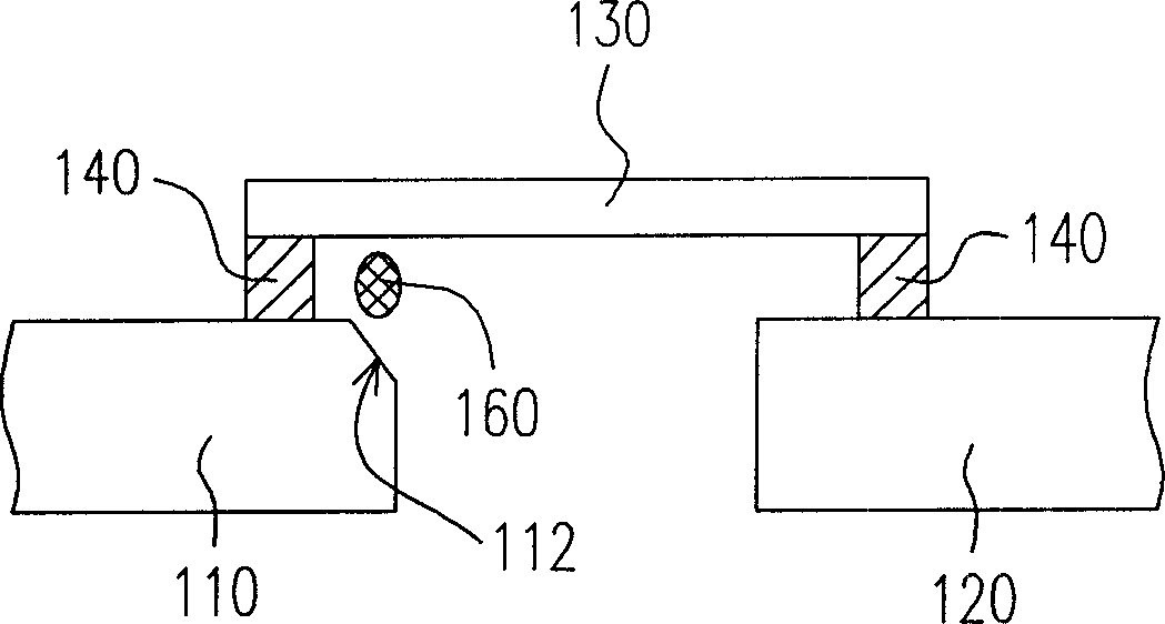
A thin-film packaging and display technology, which is applied to static indicators, instruments, identification devices, etc., can solve problems such as abnormal electrical short circuit between the packaging structure 130 and the display panel 110, and achieve the effect of prolonging the service life and improving the manufacturing qualification rate.

Inactive Publication Date: 2007-01-17
CHUNGHWA PICTURE TUBES LTD
View PDF0 Cites 7 Cited by
  • Summary
  • Abstract
  • Description
  • Claims
  • Application Information

AI Technical Summary

Problems solved by technology

[0008] However, because of this, there is a large space near the bonding area between the display panel 110 and the anisotropic conductive film 140, so the foreign matter 160 is easy to

Method used


Image

  • Display-device and thin-film packing structure
  • Display-device and thin-film packing structure
  • Display-device and thin-film packing structure

Examples


no. 1 example

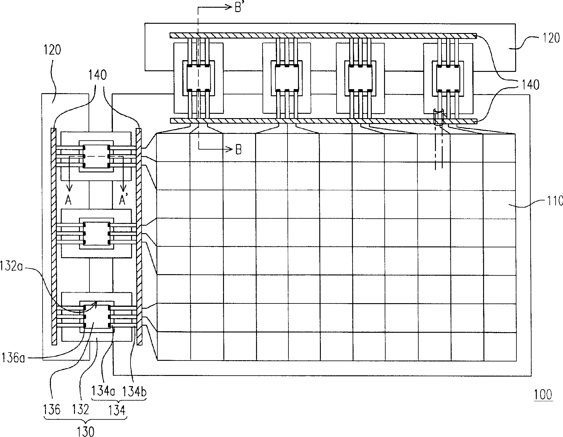
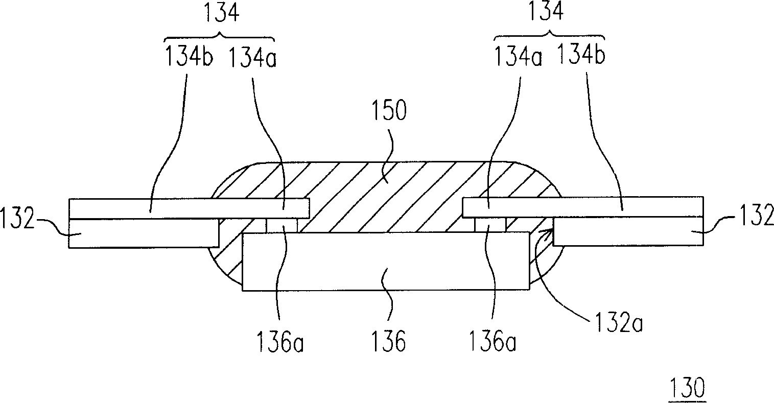
[0085] Figure 4 It is a schematic top view of a display in a preferred embodiment of the present invention. Please refer to Figure 4 , the display 200 includes a display panel 210 , a circuit board 220 and a thin film encapsulation structure 230 . Wherein, the display panel 210 has a display area 212 and a non-display area 214 . The display area 212 has a plurality of scan lines 212a and a plurality of data lines 212b, and the scan lines 212a and the data lines 212b define a plurality of pixel units 212c. If the display 200 is a liquid crystal display (liquid crystal display, LCD), each pixel unit 212c includes, for example, a thin film transistor (not shown in the figure), a liquid crystal layer (not shown in the figure) and a color filter (not shown in the figure). not shown in). The potential signal transmitted by the scan line 212a and the data line 212b can make the pixel unit 212c produce a display effect. There are some peripheral lines on the non-display area 21...

no. 2 example

[0097] Figure 9 It is a schematic diagram of a display packaged by a package structure with a chip on a flexible circuit board in another embodiment of the present invention. Please refer to Figure 9, the display 300 includes a display panel 310 and a packaging structure 320 (Chip On FPC, COF) with a chip on a flexible circuit board. Wherein, the display panel 310 has a display area 312 and a non-display area 314 . The display area 312 has a plurality of scan lines 312a and a plurality of data lines 312b, and the scan lines 312a and the data lines 312b define a plurality of pixel units 312c. If the display 300 is a liquid crystal display, each pixel unit 312c includes, for example, a thin film transistor (TFT) (not shown), a liquid crystal layer (not shown), and a color filter (not shown). And if the display 300 is an organic electroluminescent display (OLED), the pixel unit 312c includes, for example, an active element (not shown) and an organic electroluminescent elemen...


PUM


Abstract

A kind of display includes a display panel, a circuit panel and a film encapsulation structure. The circuit is at the side of the display panel. The film encapsulation structure includes a base plate, several leading feet, a chip and a prominence. The base plate has a hatch and is set between the display panel and the circuit panel. The leading feet are on the base plate and around the hatch. Every leading foot has an inner leading foot and an outer leading foot. Some outer leading feet are connected with the display panel and the others are connected with the circuit panel. The chip has multiple junctions and is set at the hatch. The junction is connected with the inner leading feet. The prominence is on the base plate and between the chip and the display panel. The encapsulation structure with the prominence can improve the pass percent of the display panel.

Description

technical field [0001] The present invention relates to a display, in particular to a display using a thin film packaging structure (TapeCarrier Package, TCP) or a packaging structure in which a chip is fixed on a flexible circuit board (Chipon FPC, COF). Background technique [0002] With the rapid development of video technology, various displays have also been developed. Generally speaking, a display has a display panel for displaying information, and the display panel is controlled by a circuit board, and the chip on the circuit board operates and provides digital signals to control each pixel on the display panel The display effect of the unit and then generate the picture. However, between the circuit board and the display panel, a packaging structure needs to be used to electrically connect the two. [0003] The thin film package structure (tape carrier package, TCP) or the chip fixed on the flexible circuit board (chip-on-FPC, COF) package structure is an optimized...

Claims


Application Information

Patent Timeline
IPC IPC(8): G02F1/133G02F1/1333G09F9/35
Inventor 陈伯龙
Owner CHUNGHWA PICTURE TUBES LTD
Why Eureka
Try Eureka