Through type photoelectric diode of low parasitic capacitance structure
A photodiode and through-type technology, which is applied in the direction of circuits, electrical components, semiconductor devices, etc., and can solve problems such as packaging of difficult automatic wiring equipment
- Summary
- Abstract
- Description
- Claims
- Application Information
AI Technical Summary
Problems solved by technology
Method used
Image

Examples
Embodiment Construction
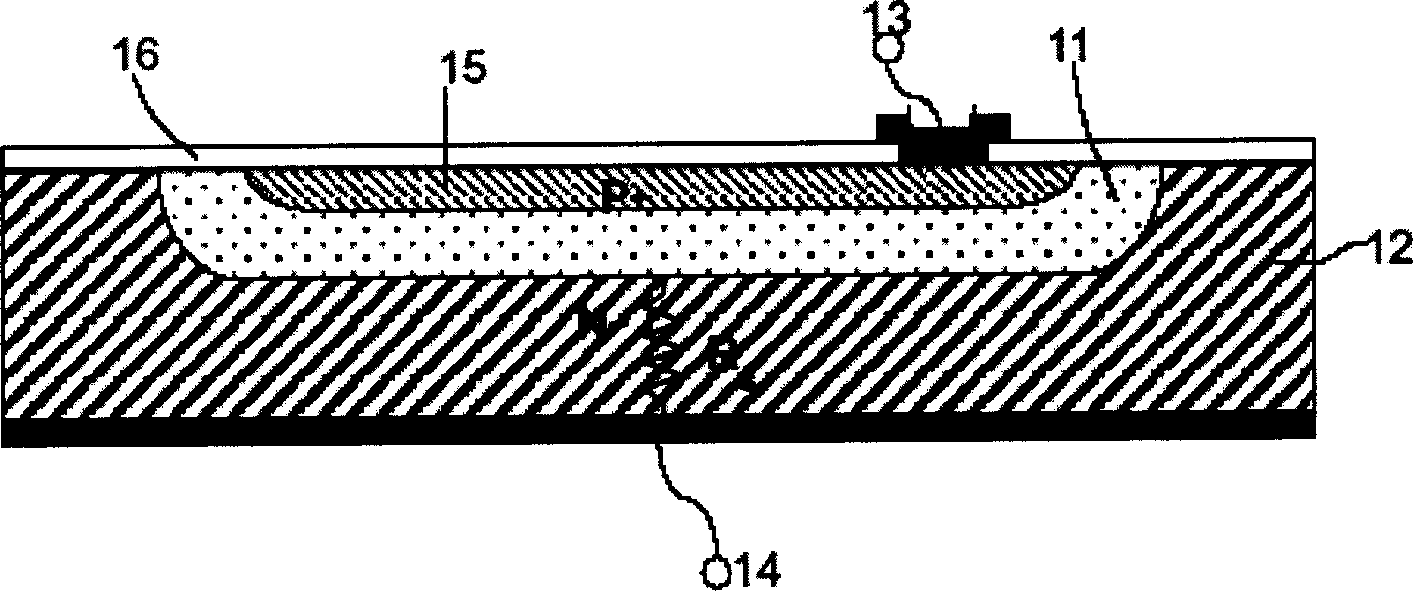
[0032] The content of the present invention can be revealed through the description of the following embodiments in conjunction with the relevant drawings. refer to Figure 4 , Figure 4is the structure of a high-speed photodiode according to an embodiment of the present invention. This photodiode is made on a silicon substrate 12, which is, for example, an N-type silicon chip with high resistivity, but it can also be a P-type, and its doping is low enough to be close to the degree of intrinsic semiconductor, so that the penetrating depletion region can be deeper to reduce junction capacitance. A heavily doped P+ layer is formed on the active region of each photodiode by diffusion or ion distribution to form the upper electrode 42 and form a PN junction with the N-type substrate. Then plate a layer of passivation glass or insulating layer 46, open a contact window in the active area with the protective layer 46 and form an active area wiring pad 41 with metal, this active a...
PUM
 Abstract
Description
Claims
Application Information
 - R&D
- Intellectual Property
- Life Sciences
- Materials
- Tech Scout
- Unparalleled Data Quality
- Higher Quality Content
- 60% Fewer Hallucinations
Browse by: Latest US Patents, China's latest patents, Technical Efficacy Thesaurus, Application Domain, Technology Topic, Popular Technical Reports.
© 2025 PatSnap. All rights reserved.Legal|Privacy policy|Modern Slavery Act Transparency Statement|Sitemap|About US| Contact US: help@patsnap.com