Static random access memory and operation method

A technology of static random access and operation method, applied in static memory, digital memory information, information storage and other directions, can solve problems such as disappearance, and achieve the effect of increased function, fast operation, and favorable integration.

Inactive Publication Date: 2007-02-21
POWERCHIP SEMICON CORP
View PDF0 Cites 0 Cited by
  • Summary
  • Abstract
  • Description
  • Claims
  • Application Information

AI Technical Summary

Problems solved by technology

Therefore, when the power supply to the memory is removed, the data stored in the SRAM will completely disappear

Method used


Image

  • Static random access memory and operation method
  • Static random access memory and operation method
  • Static random access memory and operation method

Examples


Embodiment Construction

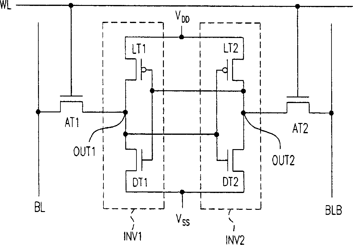
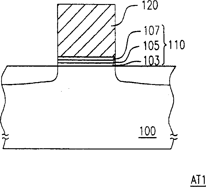
[0046] figure 1 A schematic circuit diagram of a static random access memory according to a preferred embodiment of the present invention is shown. figure 2 express figure 1 A cross-sectional view of the structure of the access transistor in .

[0047] Please refer tofigure 1 and figure 2 . The SRAM at least includes access transistors AT1 and AT2 , an inverter INV1 and an inverter INV2 . Wherein the access transistor AT1 is formed from the surface of the substrate 100, at least for example, by the bottom dielectric layer 103, the charge blocking layer 105, the top dielectric layer 107, and the gate 120 (such as figure 2 shown). Since the charge blocking layer 105 can be used to store charges, the access transistor AT1 can store data in the SRAM, so that the data will not be lost due to power interruption. The material of the bottom dielectric layer 103 and the top dielectric layer 107 is, for example, silicon oxide, and the material of the charge blocking layer 105 i...


PUM


Abstract

A storage of static random access is prepared as forming the first access transistor by bottom dielectric layer, electric charge blocking layer, top dielectric layer and grid; using electric charge blocking layer to store data of said storage for holding data not to be disappeared when power supply is interrupted, starting up the first inverter selectively as per operation of the second access transistor and starting up the second inverter selectively as per operation of the first access transistor.

Description

technical field [0001] The present invention relates to a semiconductor device, and in particular to a static random access memory and its operating method. Background technique [0002] Random access memory devices can be mainly classified into dynamic random access memory (DRAM) and static random access memory (SRAM). The advantages of the SRAM are fast operation and low power consumption. Compared with the DRAM, the SRAM does not need to be periodically charged and updated, and is relatively simple in design and manufacture. Therefore, SRAM is widely used in information electronic products. [0003] Since the SRAM is a volatile memory, it stores data in the conduction state of the transistors in the memory cells. Therefore, when the power supply to the memory is removed, the data stored in the SRAM will completely disappear. [0004] On the other hand, electrically erasable and programmable read-only memory (EEP 2 PROM) has the advantage of being able to store, read, ...

Claims


Application Information

Patent Timeline
IPC IPC(8): G11C11/412H01L27/11
Inventor 刘志拯
Owner POWERCHIP SEMICON CORP
Why Eureka
Try Eureka