
Wiring forming system and method

A technology of wiring and wiring patterns, applied in the field of wiring forming systems, can solve problems such as different degrees of occurrence, deformation of wiring patterns or uneven etching, and unclear specific structure of size adjustment standards, so as to ensure clearance, realize productivity, and realize quality Keep the effect

Inactive Publication Date: 2007-03-21
DAINIPPON SCREEN MTG CO LTD
View PDF1 Cites 3 Cited by
  • Summary
  • Abstract
  • Description
  • Claims
  • Application Information

AI Technical Summary

Problems solved by technology

[0007] However, in the above-mentioned existing wiring forming system, the size adjustment standard only discloses the case where the above-mentioned inverse problem is obtained by using a known mathematical method, and the specific structure of the size adjustment standard is still unclear.
[0008] In addition, in terms of actual manufacturing, for example, various defects such as deformation of the wiring pattern or uneven etching due to the proximity effect occur, but in the above-mentioned conventional wiring formation system, such defects are not taken into consideration.
In addition, this kind of defect does not occur equally to the entire area of ​​the printed substrate, and the degree of occurrence of this defect is different in each area of ​​the substrate
[0009] In view of the above-mentioned reasons, in the above-mentioned conventional wiring forming system, correction according to the size adjustment standard is difficult in practical use from the viewpoint of actual manufacturing, and it is substantially impossible to realize high-precision correction and improvement of productivity.

Method used


Image

  • Wiring forming system and method
  • Wiring forming system and method
  • Wiring forming system and method

Examples


no. 1 Embodiment approach

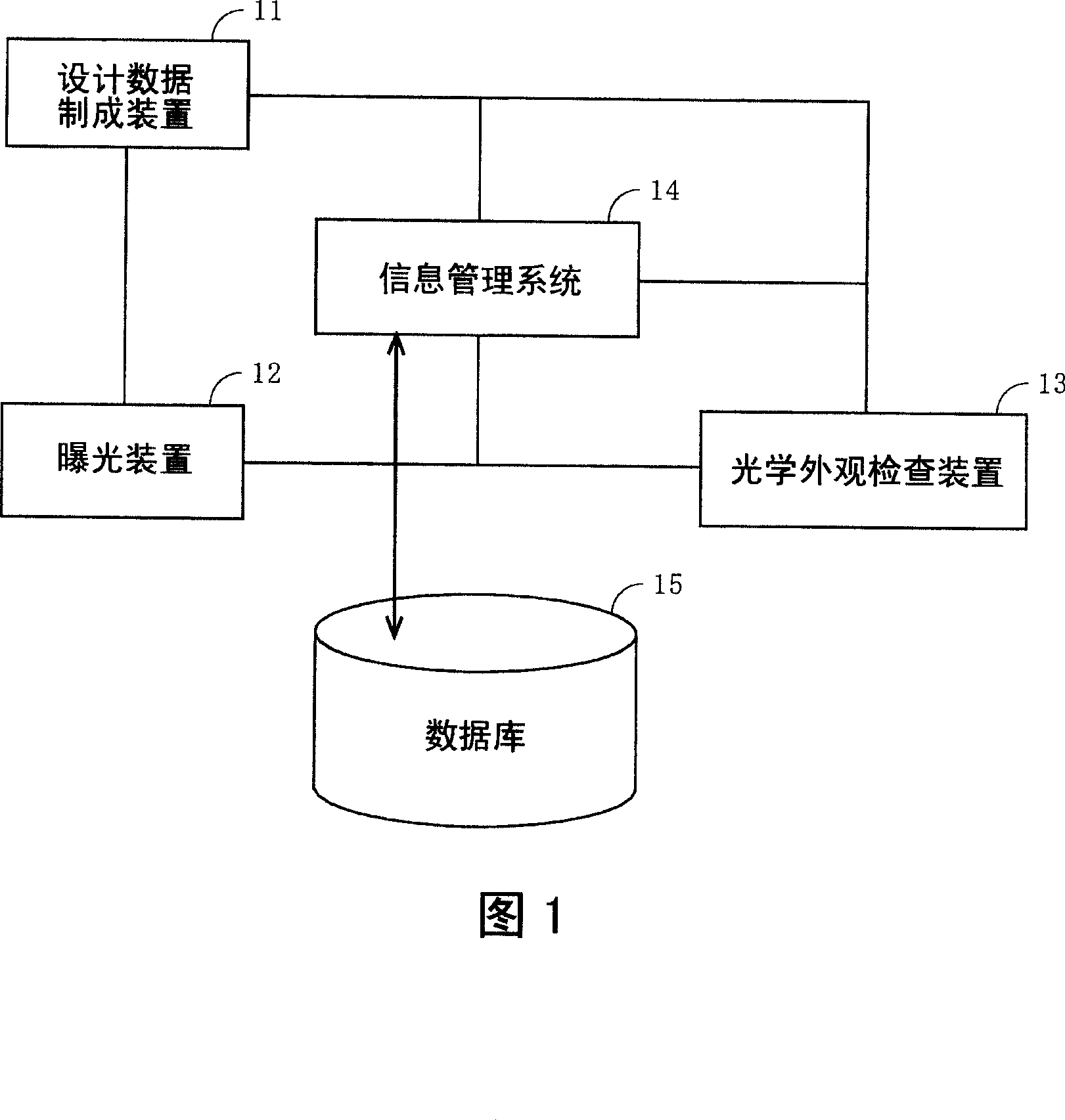
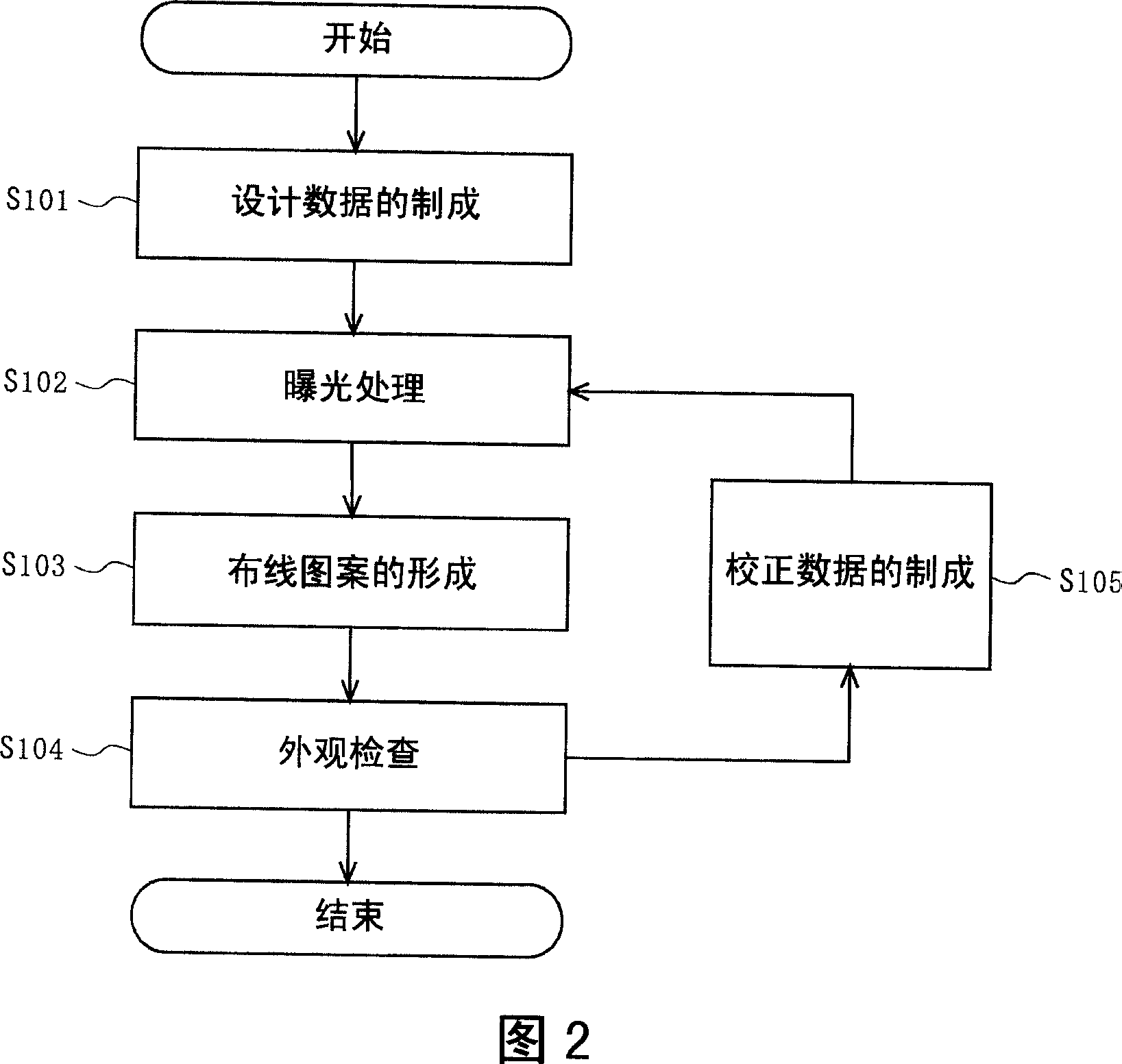
[0057] First, a wiring forming system according to a first embodiment of the present invention will be roughly described with reference to FIGS. 1 and 2 . FIG. 1 is a block diagram showing the configuration of a wiring forming system according to the first embodiment. 2 is a flowchart schematically showing the flow of processing in the wiring forming system according to the first embodiment.

[0058] In FIG. 1 , the wiring forming system according to this embodiment is a system configured by connecting a design data creating device 11 , an exposure device 12 , an optical appearance inspection device 13 , an information management system 14 , and a database 15 in a network.

[0059] In FIG. 2, the design data creating means 11 creates design data (step S101). The design data is image data representing a wiring pattern of a printed circuit board produced by CAD, CAM, or the like. The exposure device 12 creates image data for exposure (for example, RIP data) according to the de...

no. 2 Embodiment approach

[0080] Next, a wiring forming system according to a second embodiment of the present invention will be described. In this embodiment, a method of correcting defects due to the proximity effect will be described. In addition, since the wiring forming system according to this embodiment has the same configuration and processing flow as those in FIGS. 1 and 2 described in the first embodiment, description of the functions of each configuration and a rough processing flow will be omitted.

[0081] First, a defect in a wiring pattern due to the proximity effect will be described with reference to FIG. 8 . FIG. 8 is a diagram schematically showing a defect in a wiring pattern due to the proximity effect. (a) of FIG. 8 is a diagram showing a part of the wiring pattern of the mask image data. The line pitch of the two wiring patterns shown in (a) of FIG. 8 is α1. (b) of FIG. 8 is a diagram showing how a defect occurs in a wiring pattern due to the proximity effect during exposure. ...

no. 3 Embodiment approach

[0094] Next, a wiring forming system according to a third embodiment of the present invention will be described. In this embodiment, a method of correcting missing and protrusions of a wiring pattern will be described. In addition, the wiring forming system according to this embodiment is the same as the structure and process flow of FIGS. 1 and 2 described in the first embodiment except for the specific inspection method of the optical appearance inspection device 13 . Therefore, in the following description, the description of the functions of each structure other than the specific inspection method of the optical appearance inspection device 13 and a rough processing flow will be omitted.

[0095] In the present embodiment, the optical appearance inspection device 13 shown in FIG. 1 uses, for example, a plurality of cameras to photograph the printed circuit board 21 after the wiring pattern has been formed, and acquires image data of the printed circuit board 21 . The opti...


PUM


Abstract

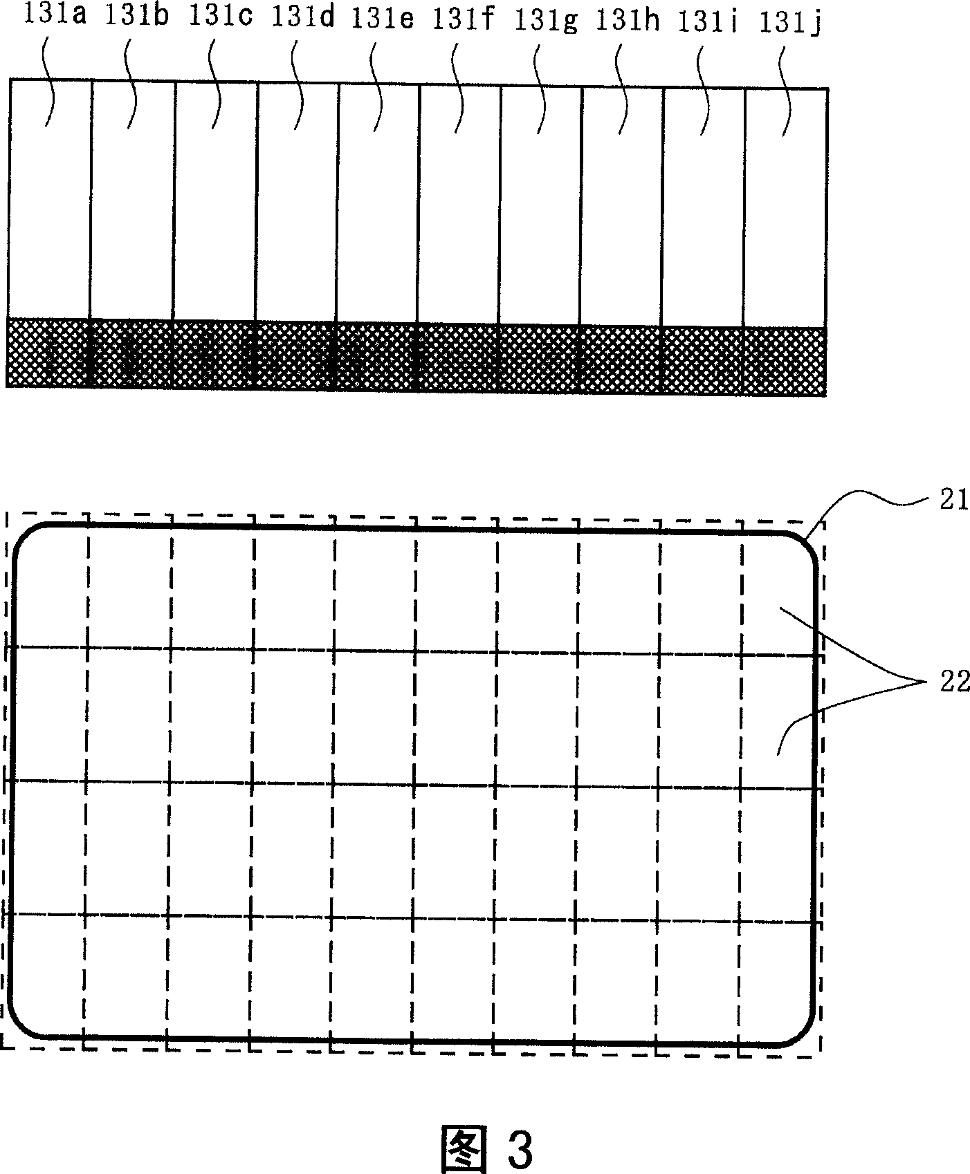
PROBLEM TO BE SOLVED: To improve the productivity of printed circuit boards by each performing highly accurate compensation on various defects generated in an actual manufacturing. ŽSOLUTION: An optical appearance inspection device 13 measures the line width of a wiring pattern using a line width measurement algorithm over the entire region of a printed circuit board after the wiring pattern is formed. Then, the optical appearance inspection device 13 prepares a line width histogram in the unit of a region 22 and further prepares a line width distribution by comparing the prepared line width histogram with the line width histogram of a master image data in the same region 22. Information management system 14 prepares a compensated data based on an average of the line width distribution prepared in a predetermined number of printed circuit boards. A stepper 12 performs a thickening or thinning compensation the line width of a wiring pattern on a design data or an image data for exposure in the unit of the region 22 based on the compensated data. Ž

Description

technical field [0001] The present invention relates to a wiring forming system and method thereof, in particular to a wiring forming system for forming a wiring pattern of a printed substrate. Background technique [0002] The wiring pattern of the printed circuit board is formed through an etching process or the like. In this etching step, for example, there is a problem that the line width of the wiring pattern changes due to thick etching or thin etching. [0003] In order to solve this problem, after the etching process, check whether the wiring pattern meets the design requirements (for example, measure the length), and the worker changes the etching conditions according to the inspection result, or modifies the mask used in the exposure process before the etching process. However, every time a worker checks that a so-called defective substrate is not produced according to the design requirements, it is necessary to recreate the etching conditions or the mask, and the...

Claims


Application Information

Patent Timeline
Patent Type & Authority Applications(China)
IPC IPC(8): H05K3/06H05K3/02G03F1/36G03F1/68G03F1/70G03F7/20H05K3/00
Inventor 八坂智冈山敏之
Owner DAINIPPON SCREEN MTG CO LTD
Learn More