TFT LCD array substrate structure and its producing method
A technology of array substrate structure and manufacturing method, which is applied in semiconductor/solid-state device manufacturing, optics, instruments, etc., can solve the problems of lower aperture ratio, reduce the jump voltage, reduce the probability of signal damage, and increase the aperture ratio Effect
- Summary
- Abstract
- Description
- Claims
- Application Information
AI Technical Summary
Problems solved by technology
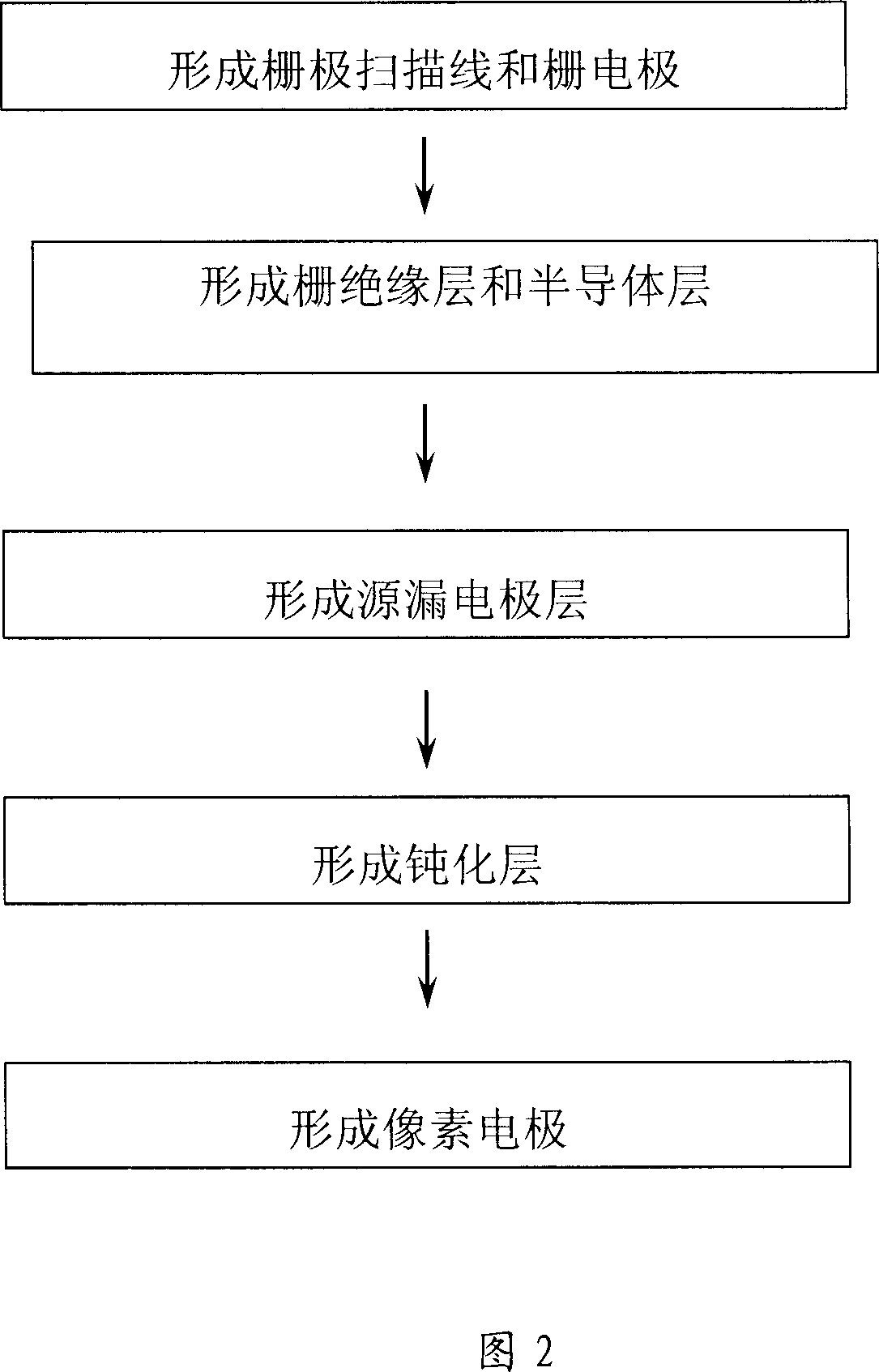
Method used
Image

Examples
Embodiment Construction
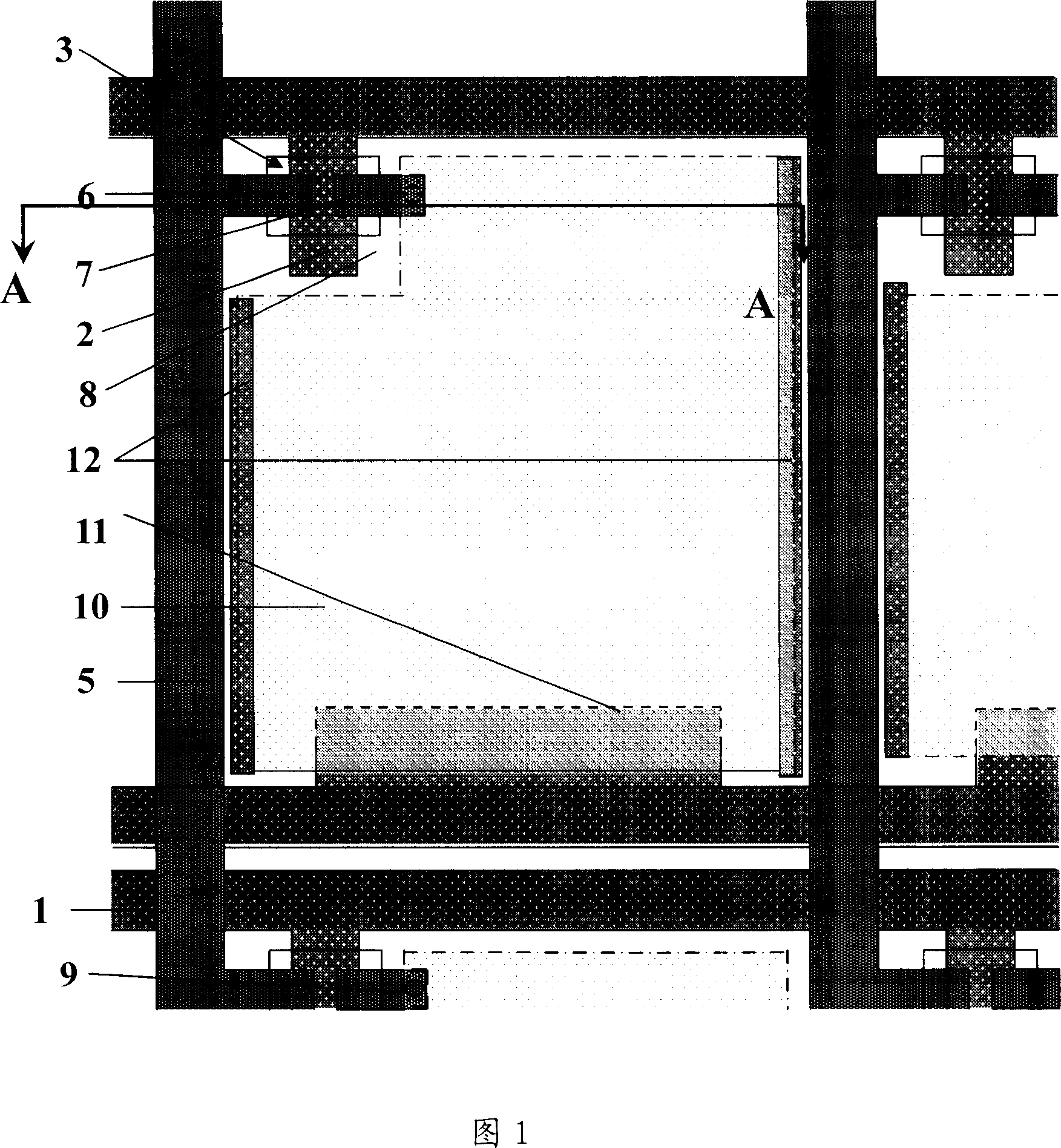
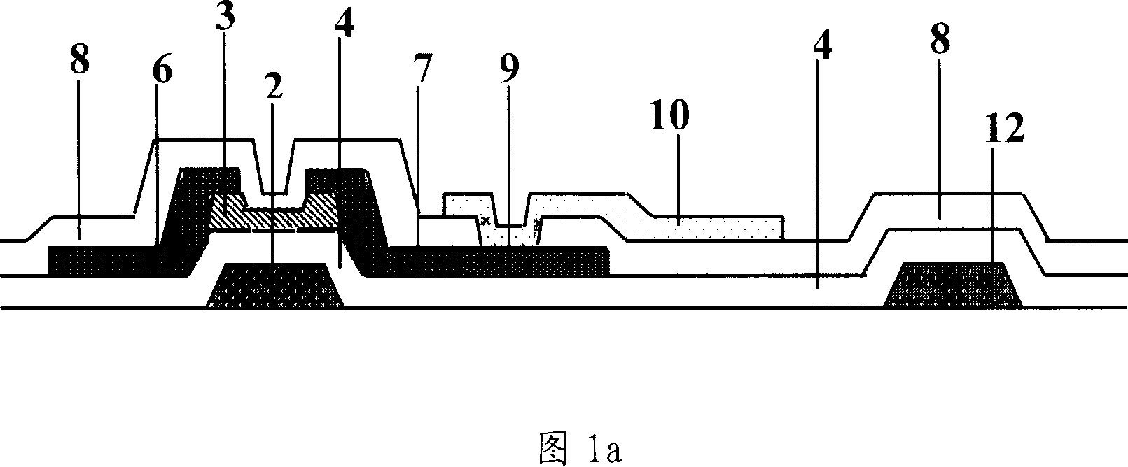
[0042]FIG. 3 is a top view of a specific embodiment of the structure of the TFT LCD array substrate of the present invention. As shown in FIG. 3 , the array substrate of the TFT LCD has a set of gate scanning lines 1 and a common electrode 13 parallel to it, and a set of data scanning lines 5 perpendicular to it. Adjacent gate scan lines 1 and data scan lines 5 define pixel regions. Each pixel includes a TFT switching device, a transparent pixel electrode 10 and a part of a common electrode 13 . As shown in FIG. 3 a , the TFT device is composed of a gate electrode 2 , a gate electrode insulating layer 4 , an active layer 3 , and a source electrode 6 and a drain electrode 7 . The transparent pixel electrode 10 is connected to the drain electrode 7 of the TFT through the passivation layer via hole 9 . The above part is the same as a conventional TFT pixel structure. The difference in the pixel structure of the TFT LCD of the present invention is that the present invention has...
PUM
 Abstract
Description
Claims
Application Information
 - R&D
- Intellectual Property
- Life Sciences
- Materials
- Tech Scout
- Unparalleled Data Quality
- Higher Quality Content
- 60% Fewer Hallucinations
Browse by: Latest US Patents, China's latest patents, Technical Efficacy Thesaurus, Application Domain, Technology Topic, Popular Technical Reports.
© 2025 PatSnap. All rights reserved.Legal|Privacy policy|Modern Slavery Act Transparency Statement|Sitemap|About US| Contact US: help@patsnap.com