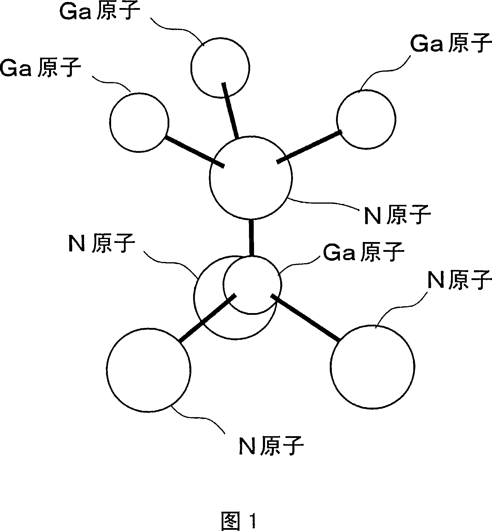
Nitride semiconductor device and method for manufacturing same
A technology of nitride semiconductor and manufacturing method, which is applied in the direction of semiconductor devices, semiconductor lasers, laser components, etc., can solve the problems of insufficient improvement of contact resistance, difficulty in manufacturing semiconductor laser devices, etc., and achieve excellent material utilization and easy cleavage , the effect of carbon concentration reduction
- Summary
- Abstract
- Description
- Claims
- Application Information
AI Technical Summary
Problems solved by technology
Method used
Image

Examples
no. 1 approach
[0056] Hereinafter, a first embodiment of a nitride semiconductor device and a method of manufacturing the same according to the present invention will be described with reference to the accompanying drawings.
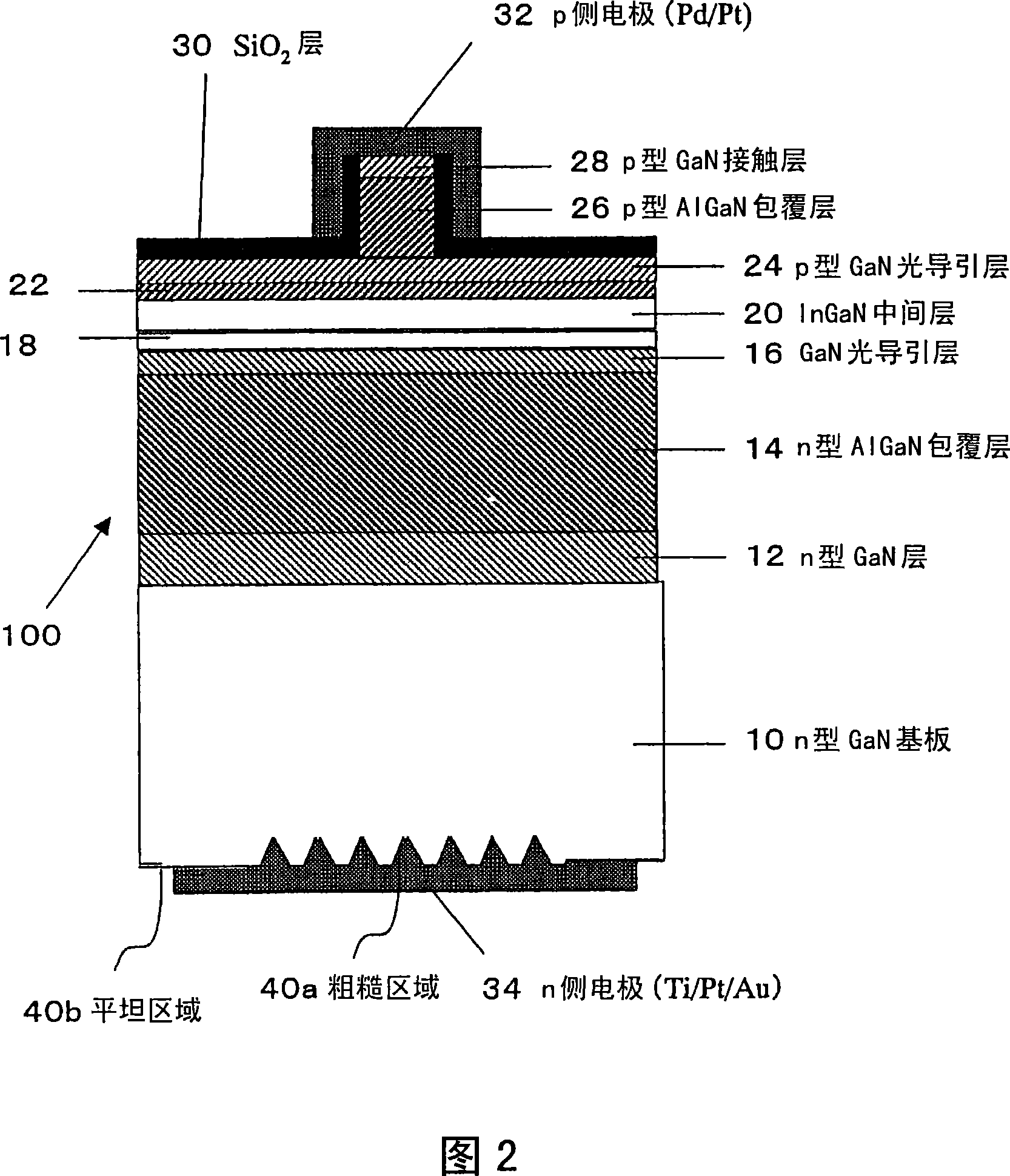
[0057] First, refer to FIG. 2 . FIG. 2 schematically shows a section of a nitride semiconductor device of this embodiment, that is, a GaN-based semiconductor laser. The element cross section shown in the figure is a plane parallel to the end face of the resonator, and the longitudinal direction of the resonator is perpendicular to the cross section.
[0058] The semiconductor laser of this embodiment includes an n-type GaN substrate (thickness: about 100 μm) 10 doped with n-type impurities, and a semiconductor stacked structure 100 provided on the surface (Ga surface) of the n-type GaN substrate 10 .
[0059] The semiconductor stacked structure 100 includes: n-type GaN layer 12, n-type AlGaN cladding layer 14, GaN optical guiding layer 16, InGaN multiple quantum well ...
Embodiment approach 2
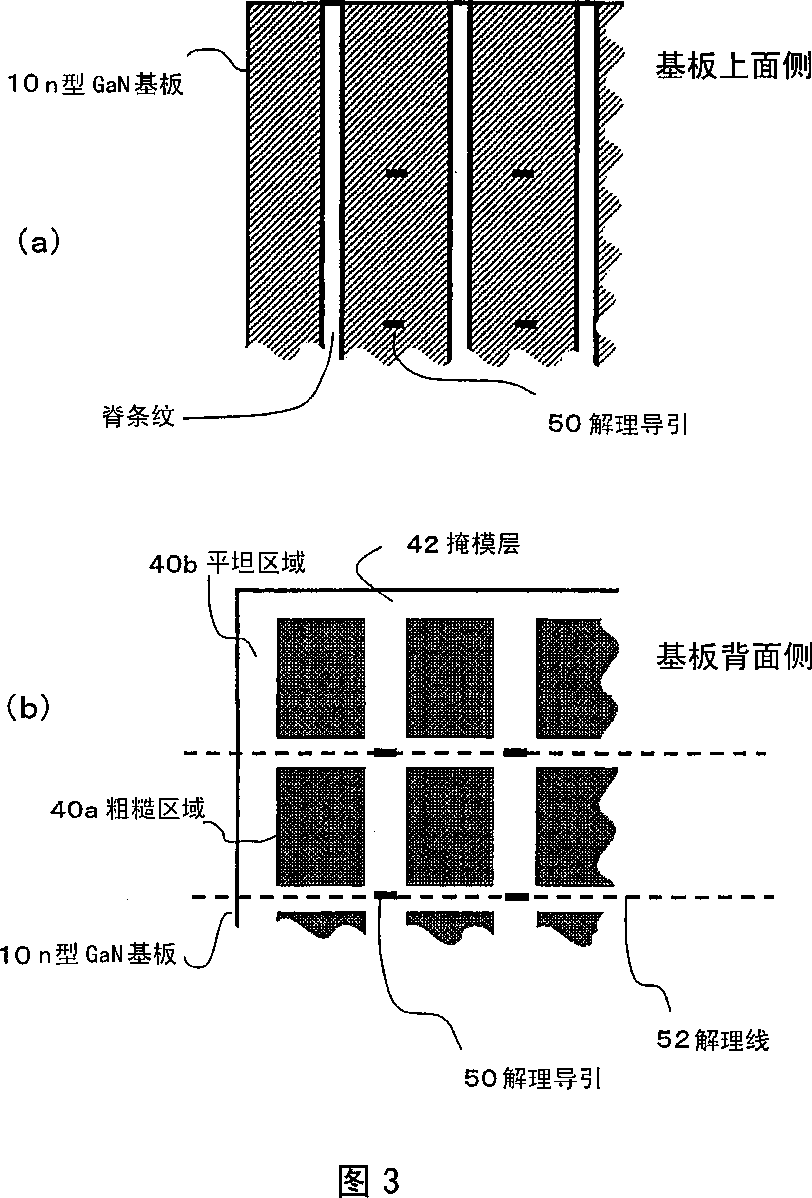
[0088] Another embodiment of the nitride semiconductor device of the present invention will be described with reference to FIGS. 6 and 7 .
[0089] The embodiment shown in FIG. 6 has the same configuration as the semiconductor laser device of Embodiment 1 except that the flat region on the back surface of the n-type GaN substrate is covered with the insulating layer 36 .
[0090] As shown in Figure 6, SiO may remain on a part of the back surface of the substrate 2 Insulating layer 36 such as film. Although it is necessary to remove the insulating film from the region where the n-side electrode 34 should be in contact with the back surface of the substrate, even if a part of the insulating film remains as the insulating layer 36 around the n-side electrode 34, it does not affect the contact characteristics. In addition, by remaining SiO on the back of the substrate 2 If the insulating layer 34 is formed such that the light (stray light) leaked from the active layer 18 to the ...
PUM
| Property | Measurement | Unit |
|---|---|---|
| Width | aaaaa | aaaaa |
| Contact resistivity | aaaaa | aaaaa |
| Thickness | aaaaa | aaaaa |
Abstract
Description
Claims
Application Information
 - Generate Ideas
- Intellectual Property
- Life Sciences
- Materials
- Tech Scout
- Unparalleled Data Quality
- Higher Quality Content
- 60% Fewer Hallucinations
Browse by: Latest US Patents, China's latest patents, Technical Efficacy Thesaurus, Application Domain, Technology Topic, Popular Technical Reports.
© 2025 PatSnap. All rights reserved.Legal|Privacy policy|Modern Slavery Act Transparency Statement|Sitemap|About US| Contact US: help@patsnap.com