Organic EL display device

A display device and organic technology, which is applied to lighting devices, electrical components, circuits, etc., can solve the problems of organic light-emitting media destroying display, prone to disconnection, and increasing cost, and achieves improved fluorescence conversion efficiency, reduced defects, and simplified structure. Effect

Inactive Publication Date: 2007-05-23
IDEMITSU KOSAN CO LTD
View PDF7 Cites 28 Cited by
  • Summary
  • Abstract
  • Description
  • Claims
  • Application Information

AI Technical Summary

Problems solved by technology

This configuration has the same problem as (1), and since a thick light-shielding layer, pillar, or stress relief layer is required, the configuration becomes complicated and the cost increases
[0011] (4) In Patent Document 5, although the columns are formed on the color conversion substrate, an overcoat layer for filling the gaps between the color conversion layers is required, and the columns cover the organic EL. In the light-emitting area, pressure will be applied to the organic light-emitting medium, so the stress caused by temperature changes may destroy the organic light-emitting medium and cause display defects
[0012] (5) In Patent Document 6, although a color conversion substrate is formed in which the color conversion layer is separated by a transparent partition wall, the organic EL is directly stacked on the color conversion substrate instead of the organic EL substrate and the color conversion substrate. Change the configuration where the substrates face each other, and the partition wall does not function as a spacer between the two
In addition, organic EL is directly affected by volatile components such as the surface smoothness of the color conversion substrate and moisture, and is prone to display defects such as disconnection, short circuit, and black spots.

Method used


Image

  • Organic EL display device
  • Organic EL display device
  • Organic EL display device

Examples


Embodiment approach 1

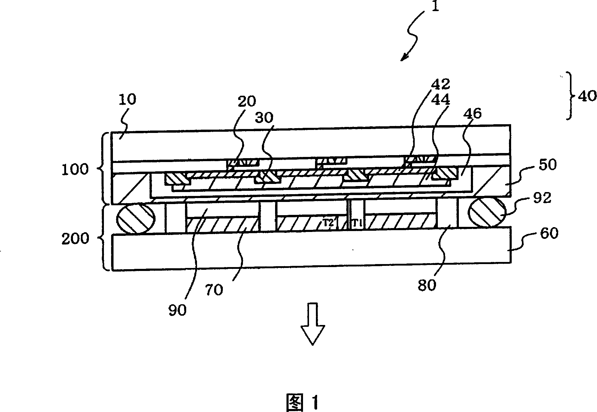
[0060] FIG. 1 shows an organic EL display device according to one embodiment of the present invention.

[0061] This organic EL display device 1 comprises an organic EL substrate 100 on which an organic EL element 40 is formed on a first substrate 10, and a color conversion substrate 200 on which a color conversion layer 70 is formed on a second substrate 60 so that the organic EL element 40 and the color The transformation layers 70 are arranged so as to face each other.

[0062] Specifically, in the organic EL substrate 100 , the TFT 20 , the interlayer insulating film 30 , the lower electrode 42 , the organic luminescent medium 44 , the upper electrode 46 , and the barrier film 50 are formed on the first substrate 10 . Here, the organic EL element 40 is constituted by the lower electrode 42 , the organic light-emitting medium 44 , and the upper electrode 46 .

[0063] In the color conversion substrate 200 , the color conversion layer 70 and the transparent partition walls ...

Embodiment approach 2

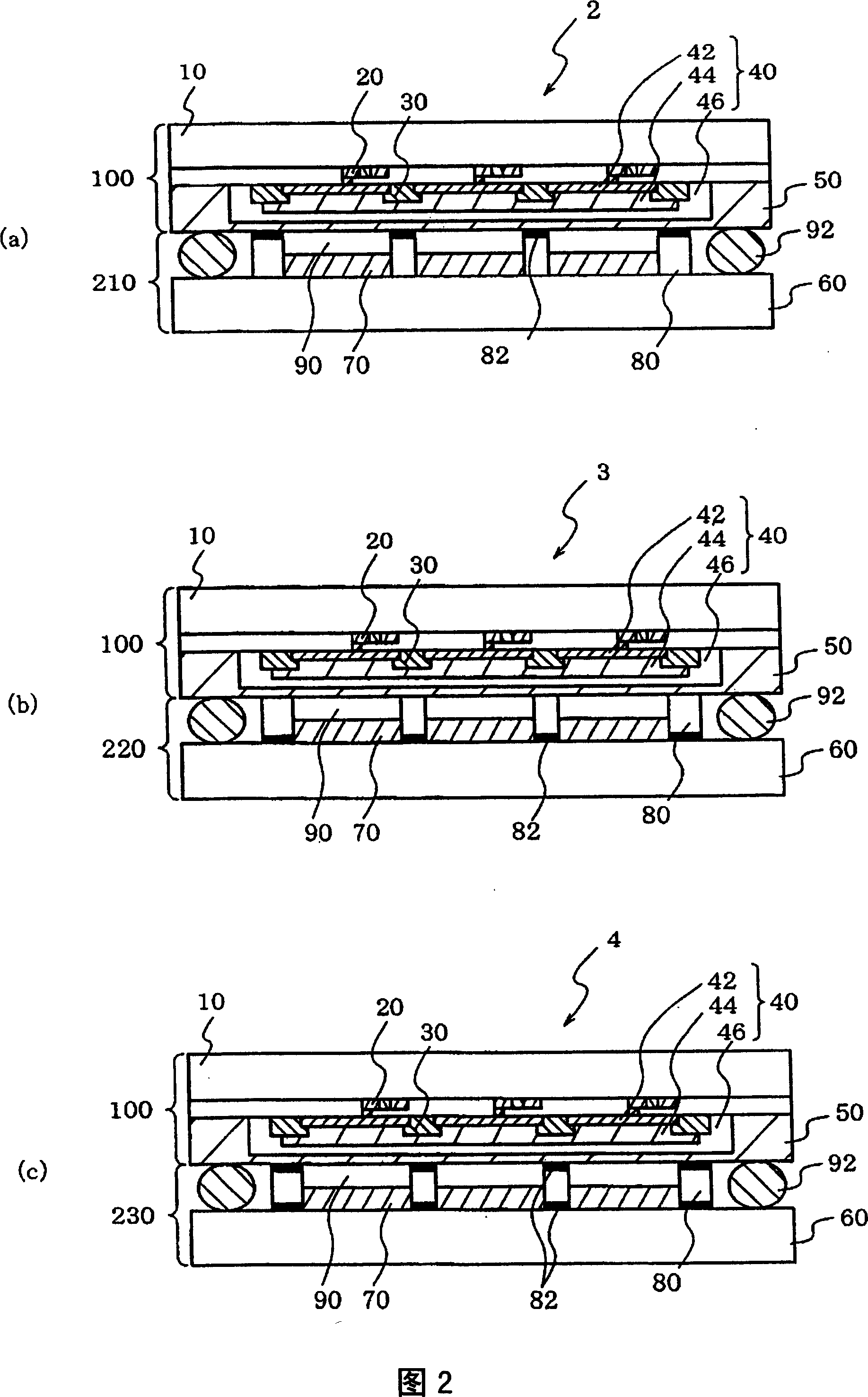
[0075] FIG. 2 shows an organic EL display device according to another embodiment of the present invention.

[0076] In addition, in the following drawings, the same reference numerals are used for the same members as those in FIG. 1 , and description thereof will be omitted.

[0077] In this embodiment, only the partition wall of the color conversion substrate is different from the first embodiment.

[0078] In the organic EL display device 2 of FIG. 2( a ), a light shielding layer 82 is formed on the upper portion of the partition wall 80 of the color conversion substrate 210 .

[0079] In the organic EL display device 3 of FIG. 2( b ), a light shielding layer 82 is formed on the lower portion of the partition wall 80 of the color conversion substrate 220 .

[0080] In the organic EL display device 4 of FIG. 2( c ), light shielding layers 82 are formed on the lower and upper portions of the partition walls 80 of the color conversion substrate 230 .

[0081] By forming the l...

Embodiment approach 3

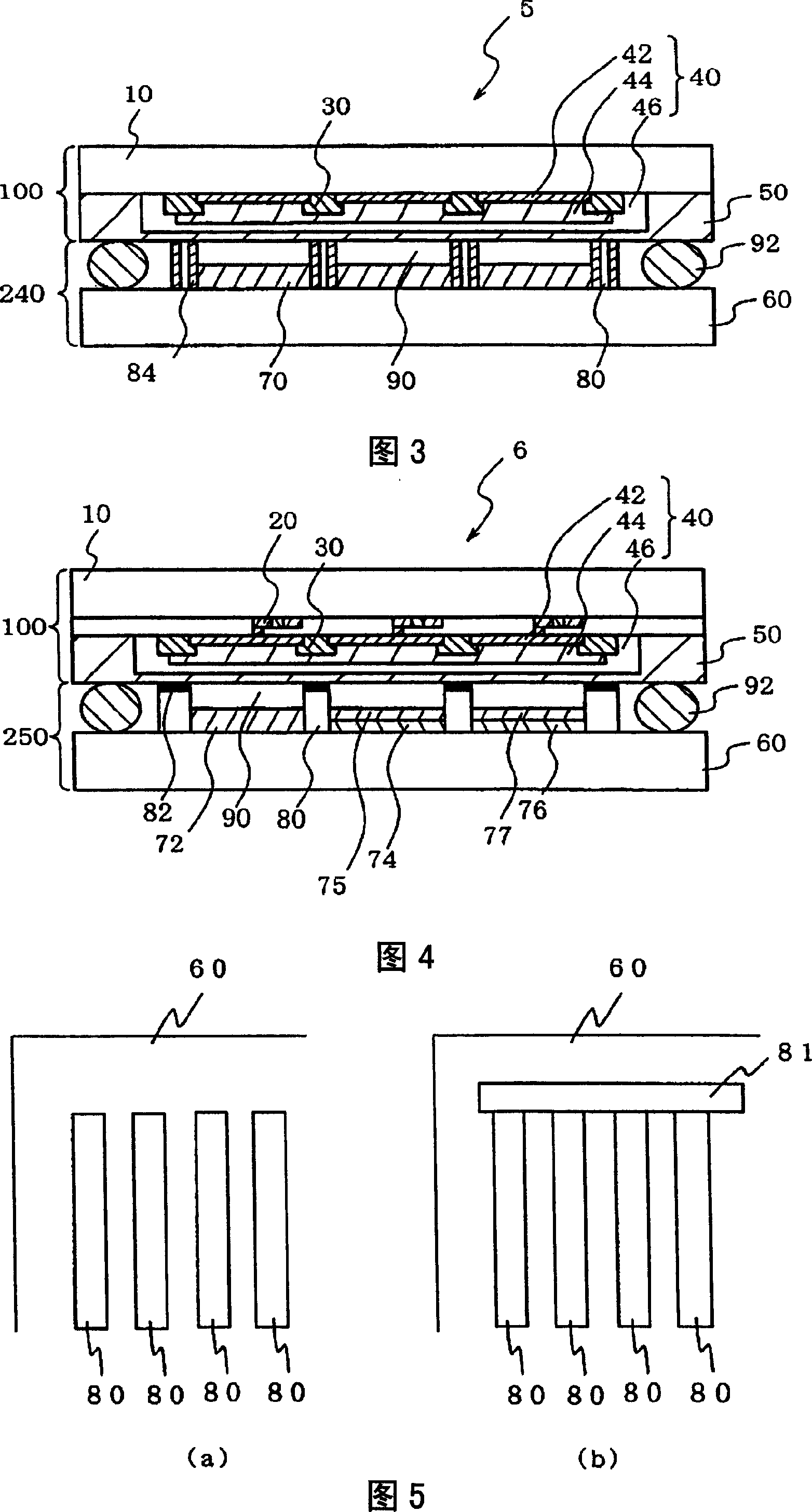
[0083] FIG. 3 shows an organic EL display device according to another embodiment of the present invention.

[0084] In this embodiment, only the partition wall of the color conversion substrate is different from the first embodiment.

[0085] In the organic EL display device 5 of FIG. 3 , a reflective layer 84 having a function of reflecting visible light is formed on the side of the partition wall 80 of the color conversion substrate 240 .

[0086] The light emitted from the color conversion layer 70 is reflected by the reflective layer 84 and is effectively used for display of the organic EL display device. Moreover, in order to reflect visible light not only with the reflective layer but also with the side walls of the partition walls, the side surfaces may be roughened, and particles having a refractive index different from those of the partition walls may be dispersed in the partition walls to the extent that the transparency of the partition walls is not lost to scatter ...


PUM


Abstract

In an organic EL display device, an organic EL board (100) wherein an organic EL element (40) is formed on a first board (10), and a color conversion board (200) wherein a color conversion layer (70) is formed on a second board (60) are arranged by permitting the organic EL element (40) to face the color conversion layer (70). A transparent wall (80) which is thicker than the color conversion layer (70) is provided between the color conversion layers (70) of the color conversion board (200). The wall (80) is a partition wall for separating the color conversion layer (70), and is also a spacer between the organic EL board (100) and the color conversion board (200). A sealing medium (90) is provided between the walls (80) with the color conversion layer (70).

Description

technical field [0001] The present invention relates to an organic electroluminescence (EL) display device, in particular to an organic EL display device provided with a color conversion layer. Background technique [0002] In recent years, various flat-panel displays (flat-panel display devices) such as liquid crystal display devices (LCD) have been developed. Among these flat panel displays, the EL display device has high visibility because it is self-luminous, and is excellent in impact resistance because it is completely solid. In an EL display device, a voltage is applied between two electrodes provided to sandwich a light emitting layer containing an organic compound, an inorganic compound, etc., and a current flows to cause the light emitting layer to emit light. [0003] As one of full-colorization methods of an EL display device, there is a method in which a fluorescent material layer absorbs EL light incident from a light-emitting layer and emits fluorescence (col...

Claims


Application Information

Patent Timeline
Patent Type & Authority Applications(China)
IPC IPC(8): H05B33/04H05B33/12H05B33/14
CPCH01L51/5275H01L51/5271H01L27/3244H01L27/322H01L51/5237H01L51/5284H10K59/38H10K59/12H10K50/8428H10K50/8426H10K50/858H10K50/856H10K50/865H05B33/04H05B33/14
Inventor 荣田畅福田雅彦
Owner IDEMITSU KOSAN CO LTD
Why Eureka
Try Eureka