Method for making thick metal inductance in integrated circuit

A manufacturing method and integrated circuit technology, applied in the manufacture of circuits, electrical components, semiconductors/solid-state devices, etc., can solve problems such as sidewall corrosion of metal lines, voids, and inability to meet the etching requirements of thick metal layers, and achieve good electrical properties , Good process stability

Active Publication Date: 2007-06-13
SHANGHAI HUAHONG GRACE SEMICON MFG CORP
View PDF0 Cites 9 Cited by
  • Summary
  • Abstract
  • Description
  • Claims
  • Application Information

AI Technical Summary

Problems solved by technology

In the existing 0.25um MOS integrated circuit, the thickness of the usual top layer metal film is about 8000 angstroms. Since it will also be used as an inductor, a thick metal film must be used in order to obtain low resistivity. The process gas, flow rate and time used for etching in the prior art Process parameters such as power and power will not be able to meet the etching requirements of thick metal layers; second, the wet cleaning process after etching
Due to the use of a thick metal film, the thickness of the corresponding photoresist must be thickened during etching, which leads to a large increase in the polymer produced during the etching process, which brings great difficulty to the subsequent cleaning steps. The choice of cleaning solution And a reasonable cleaning time is extremely important. Using the existing cleaning process may cause the polymer to be cleaned uncleanly, or excessive cleaning may cause the sidewall of the metal line to be corroded and form a cavity, which will affect the reliability of the interconnection and the performance of the inductance.

Method used


Image

  • Method for making thick metal inductance in integrated circuit
  • Method for making thick metal inductance in integrated circuit

Examples


Embodiment Construction

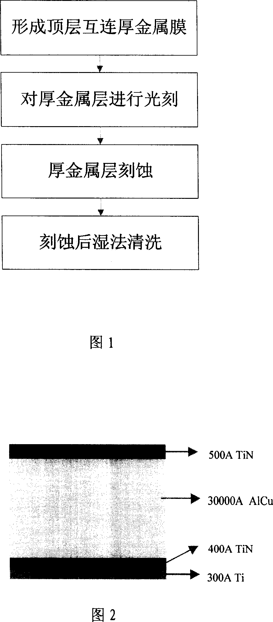
[0012] FIG. 1 is a schematic flow chart of a method for manufacturing a thick metal inductor in an integrated circuit according to the present invention. As shown in FIG. 1 , the present invention first adopts physical vapor deposition to sequentially deposit 300 angstrom Ti / 400 angstrom TiN / 30000 angstrom AlCu / 500 angstrom TiN to form a 3 micron thick top layer interconnect thick metal film. Wherein, the schematic diagram of the structure of the thick metal layer is shown in FIG. 2 . Second, the thickness of AlCu can be 28000 angstroms to 32000 angstroms. A photoresist with a thickness of 4.0um is used as the metal pattern protective layer during etching. The third step, with Cl 2 and BCl 3 The thick metal layer is etched by dry etching method as the main etching gas, and the type of etching equipment used is DPS CENTURA5200 of Applied Materials for dry etching, and the dry etching is divided into three steps. Its process parameters are shown in Figure 5. First, it is the...


PUM

PropertyMeasurementUnit
thicknessaaaaaaaaaa
thicknessaaaaaaaaaa

Abstract

The method includes steps: (1) using physical vapor deposition to deposit Ti, TiN, AlCu, and TiN in sequence to form thick metal films interlinked through top level; (2) using thick photoresist as metal graph protection layer in etching time to carry out photo etching for thick metal layers; (3) using Cl2 and BCl3 as main etching gases, the dry etching method carries out etching for thick metal layers; (4) using wet cleaning process to carry out cleaning step after etching. The invention is suitable to IC-manufacture area.

Description

technical field [0001] The invention relates to a method for manufacturing a metal inductor in an integrated circuit, in particular to a method for manufacturing a thick metal inductor in an integrated circuit. Background technique [0002] In radio frequency integrated circuits, it is necessary to use thick top-layer interconnection metals as inductive materials to make integrated circuit inductive components. However, the fabrication of thick metal inductors needs to overcome the following points in the prior art: first, the etching of the thick metal layer. In the existing 0.25um MOS integrated circuit, the thickness of the usual top layer metal film is about 8000 angstroms. Since it will also be used as an inductor, a thick metal film must be used in order to obtain low resistivity. The process gas, flow rate and time used for etching in the prior art Process parameters such as power and power will not be able to meet the etching requirements of thick metal layers; seco...

Claims


Application Information

Patent Timeline
Patent Type & Authority Applications(China)
IPC IPC(8): H01L21/768H01L21/3213
Inventor 姚泽强金炎俞波
Owner SHANGHAI HUAHONG GRACE SEMICON MFG CORP
Why Eureka
Try Eureka