Production of semiconductor anti-reflective layer

An anti-reflection layer and a manufacturing method are applied in the manufacture of semiconductor/solid-state devices, the photoengraving process of the pattern surface, optics, etc., to achieve the effect of high wet method selection ratio and simple and easy method.

Inactive Publication Date: 2007-06-20
SHANGHAI HUA HONG NEC ELECTRONICS
View PDF0 Cites 4 Cited by
  • Summary
  • Abstract
  • Description
  • Claims
  • Application Information

AI Technical Summary

Problems solved by technology

And for NH 3 ARL, this method is not applicable, because this ARL has to take into account the SiO 2 The wet high selectivity ratio

Method used


Image

  • Production of semiconductor anti-reflective layer
  • Production of semiconductor anti-reflective layer

Examples


Embodiment Construction

[0012] The manufacturing method of the semiconductor anti-reflection layer of the present invention includes two steps of growth and photolithography of the anti-reflection layer in the prior art, and between the two steps of growth of the anti-reflection layer and photolithography, an anti-reflection layer is added. O 2 Steps of plasma treatment. in progress 2 During plasma treatment, the RF (radio frequency) power is 500-2000 watts, O 2 The flow rate is 200~2000sccm, and the gas pressure is 0.1~2Torr. If the antireflection layer of silicon nitride in the field area is O 2 Plasma treatment, the treatment time is 10 ~ 60S; if the antireflection layer of the gate polysilicon is O 2 Plasma treatment, the treatment time is 10 ~ 60S.

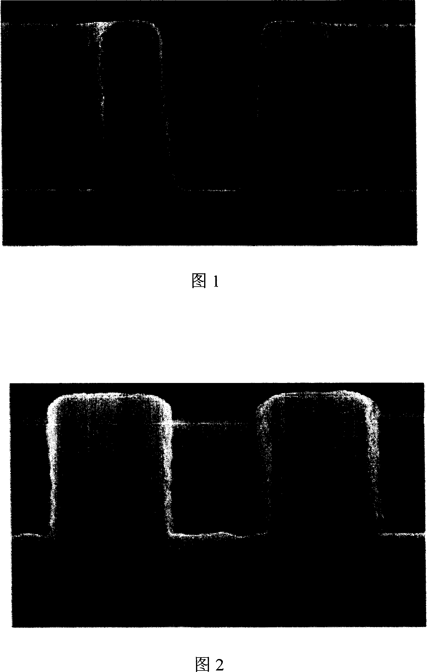
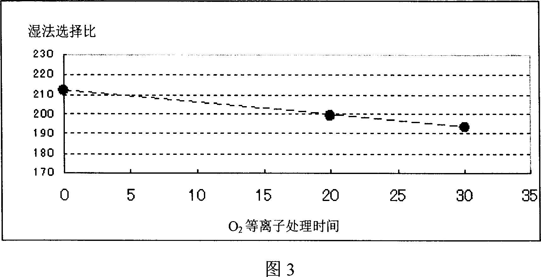
[0013] By processing the anti-reflection layer with the method of the present invention, the resulting footing or scumming phenomenon is greatly improved, as can be seen in FIG. 2 . In addition, after O 2 After plasma treatment, the wet etch ...


PUM


Abstract

The invention is concerned with the manufacture method of semiconductor anti-reflection layer, includes two steps that are the growth and the photo-etching of the anti-reflection layer, and a step that processes O2 plasma processing to the anti-reflection layer between the growth and the photo-etching steps. The invention can remove the footing or scumming phenomenon that creates by the direct touch of SiON and the DUV photo-etching pastern on the ARL with NH3, and have higher aqueous wet method selective rate for SiO2.

Description

technical field [0001] The invention relates to a manufacturing method of a semiconductor anti-reflection layer. Background technique [0002] The existing process for making the anti-reflection layer is to directly perform the photolithography process after the anti-reflection layer is formed. The ARL (anti-reflection layer) grown by enhanced chemical vapor deposition is generally divided into two types of reaction gases: one reaction gas is mainly composed of SiH 4 and N 2 Composed of O, this gas is generally used in the process of aluminum layer or through hole, which can reduce metal reflection and enhance the CD (strip width) stability of subsequent photolithography engineering; another reaction gas is mainly composed of SiH 4 , N 2 O and NH 3 Composed of, with ordinary SiH 4 and N 2 Compared with the SiON generated by the O reaction, the SiON formed due to this gas is more effective than the HDP (High Density Plasma)-SiO used in the device isolation STI (Shallow ...

Claims


Application Information

Patent Timeline
Patent Type & Authority Applications(China)
IPC IPC(8): H01L21/027H01L21/31G03F7/00
Inventor 王剑敏
Owner SHANGHAI HUA HONG NEC ELECTRONICS
Why Eureka
Try Eureka