Method for ion implantation of high-voltage transistor LDD

A high-voltage transistor and ion implantation technology, which is applied in semiconductor/solid-state device manufacturing, electrical components, circuits, etc., can solve the problems of poor reliability and the inability of transistors to further increase the breakdown voltage, so as to reduce hot carriers effect, improve reliability, and increase breakdown voltage

Inactive Publication Date: 2007-06-20
SHANGHAI HUA HONG NEC ELECTRONICS
View PDF0 Cites 5 Cited by
  • Summary
  • Abstract
  • Description
  • Claims
  • Application Information

AI Technical Summary

Problems solved by technology

Transistors made by this method cannot further increase their breakdown v

Method used


Image

  • Method for ion implantation of high-voltage transistor LDD
  • Method for ion implantation of high-voltage transistor LDD
  • Method for ion implantation of high-voltage transistor LDD

Examples


Embodiment Construction

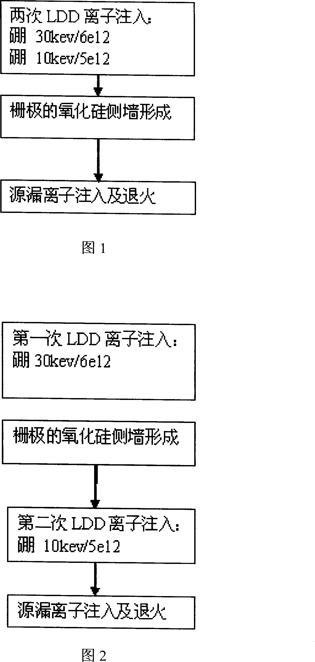
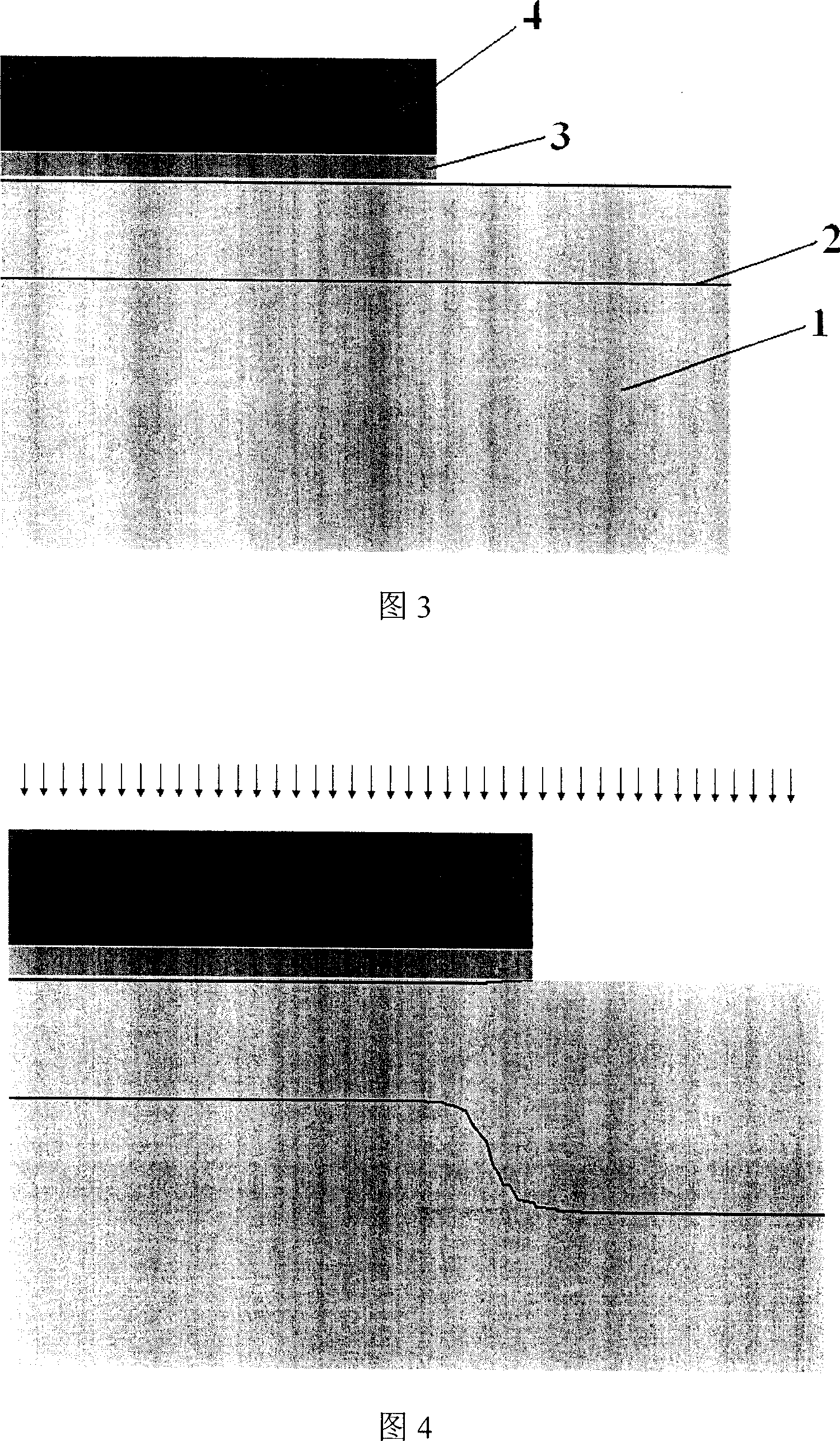
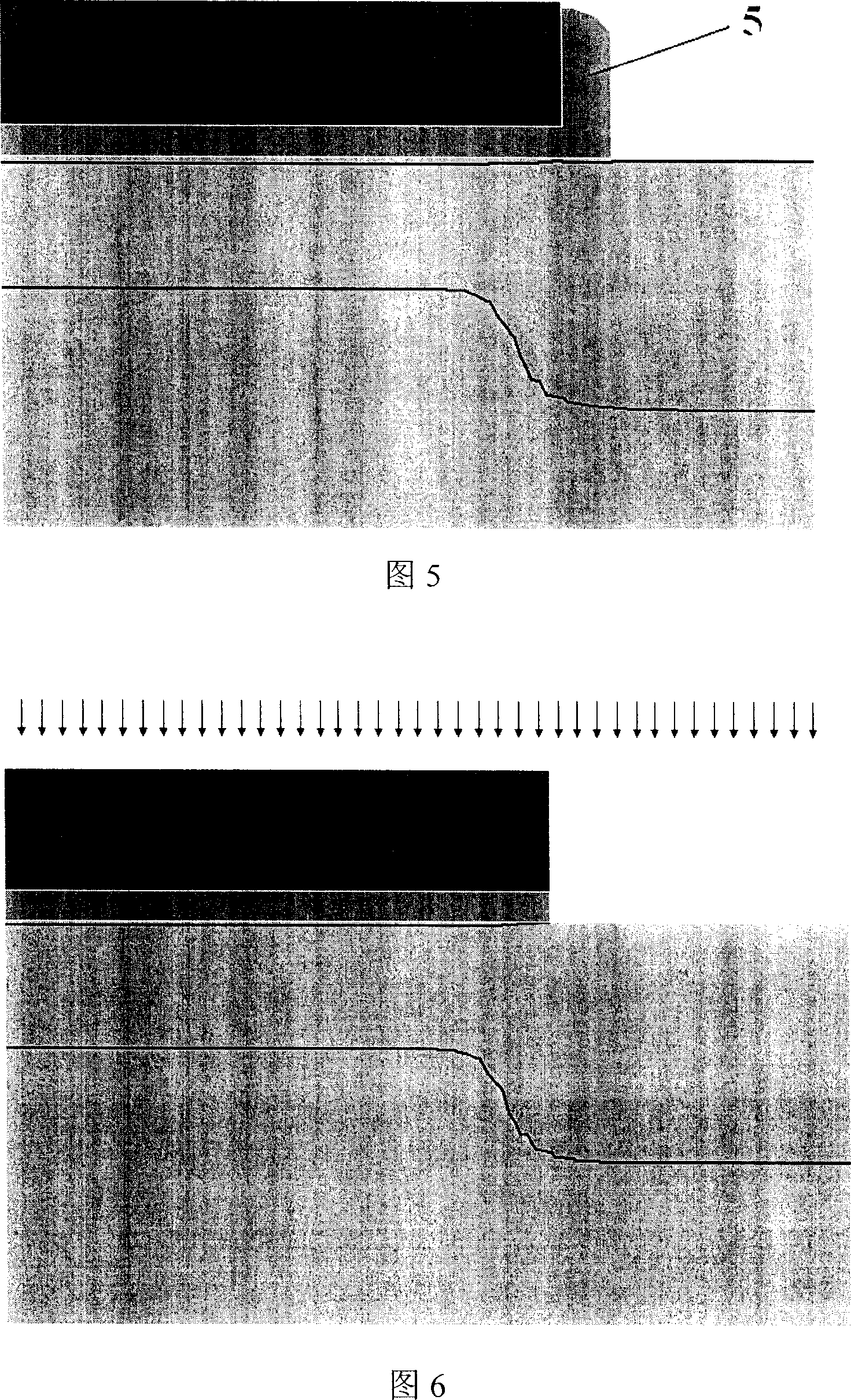
[0024] The flow chart of the LDD ion implantation method of the high-voltage transistor of the present invention can be seen in FIG. 2, which specifically includes four steps. FIG. 3 shows a device structure that has not been ion implanted, which includes the underlying silicon substrate 1, gate silicon oxide 3, and polysilicon 4. For this device, the first LDD ion implantation is performed, the implanted element is boron, the implanted boron dose is 30keV, and the energy is 6e12. After this step, the PN junction interface 2 will be deformed, as shown in FIG. 4. Then the silicon nitride sidewall spacer 5 of the gate is formed, as shown in FIG. 5. Then perform the second LDD ion implantation, the implanted element is still boron, the implanted boron dose is 10kev, and the energy is 5e12. As shown in Figure 6, the energy of this LDD ion implantation is lower than that of the first LDD ion implantation energy. Finally, source and drain ion implantation and annealing are performed. As...


PUM


Abstract

The invention is concerned with the method of high-pressured transistor LDD ion implantation, it is: separates the multi-times LDD ion implantation during the high-pressured parts technics, processes the high-energy ion implantation before forming the silicon oxidation sidewall of the grid, the low-energy ion implantation finishes after the silicon oxidation sidewall of the grid, in order that the fold area of the LDD and the grid adulterates slightly, increases the breakdown potential of the LDD knot, decreases heat carrier effect, improves the reliability of the parts, the threshold value voltage and saturation current of the parts maintains steadily because the adulterating thickness between the sidewall and the active leaking is steadiness.

Description

Technical field [0001] The invention relates to a method for ion implantation of transistors, in particular to a method for ion implantation of high voltage transistor LDD (Lightly Doped Drain, lightly doped source and drain). Background technique [0002] High-voltage devices need to have a sufficiently high breakdown voltage, so whether it is a channel or a source-drain junction, it has higher requirements for its breakdown voltage. Increasing the channel breakdown voltage can generally be accomplished by increasing the channel length, and increasing the breakdown voltage of the source-drain junction requires lightly doped source-drain (LDD) ion implantation to obtain a deeper graded junction. In the case of a certain gate length, increasing the effective channel length and deepening the LDD junction depth are contradictory. Therefore, in the design of high-voltage devices, first meet the LDD junction breakdown voltage, and then select a sufficient gate length to meet the chann...

Claims


Application Information

Patent Timeline
IPC IPC(8): H01L21/336H01L21/265
Inventor 钱文生胡君
Owner SHANGHAI HUA HONG NEC ELECTRONICS
Why Eureka
Try Eureka