Nitride semiconductor light emitting device and method of fabricating nitride semiconductor laser device
一种氮化物半导体、发光器件的技术,应用在半导体激光器、半导体/固态器件制造、半导体器件等方向,能够解决暗线退化等问题,达到提高可靠性的效果
- Summary
- Abstract
- Description
- Claims
- Application Information
AI Technical Summary
Problems solved by technology
Method used
Image

Examples
no. 1 approach
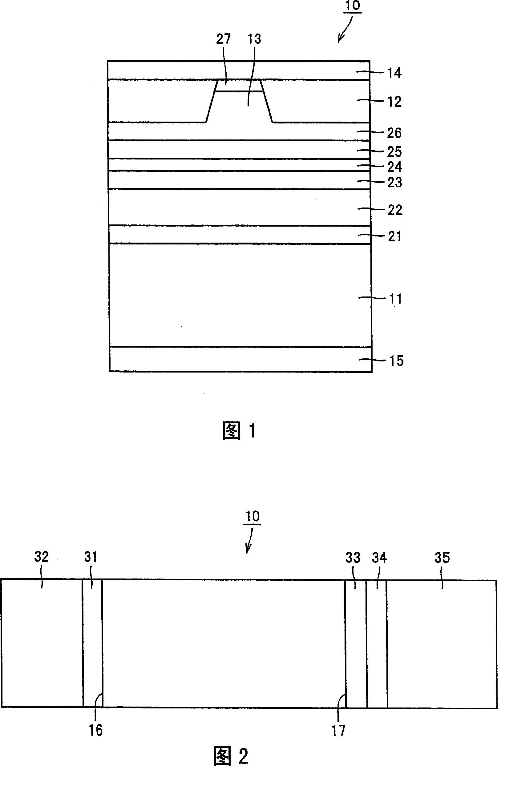
[0038] FIG. 1 is a schematic cross-sectional view of a preferred example of the nitride semiconductor laser of the present embodiment. Here, the present embodiment provides a nitride semiconductor laser 10, which includes an n-type GaN substrate 11, an n-type AlGaInN buffer layer 21 deposited on the n-type GaN substrate 11, and an n-type AlGaInN buffer layer 21 deposited on the n-type GaN substrate 11. The n-type AlGaInN cladding layer 22 on the AlGaInN buffer layer 21, the n-type AlGaInN guide layer 23 deposited on the n-type AlGaInN cladding layer 22, the AlGaInN multi-quantum well active layer 24 deposited on the n-type AlGaInN guide layer 23, deposited on A p-type AlGaInN guide layer 25 on the AlGaInN multi-quantum well active layer 24, a p-type AlGaInN cladding layer 26 deposited on the p-type AlGaInN guide layer 25, and a p-type AlGaInN contact layer 27 deposited on the p-type AlGaInN cladding layer 26 . It should be noted that each layer has a suitably adjusted composi...
no. 2 approach
[0061] The present embodiment provides a nitride semiconductor laser having a structure similar to that of the first embodiment except that the cavity has a light-emitting facet coated with a structurally modified coating film.
[0062] Here, in the present embodiment, the nitride semiconductor laser has a cavity having a light emitting facet provided with a 20 nm thick aluminum oxynitride film and a 69 nm thick aluminum oxide film deposited thereon to produce 5 % reflectance. Note that the aluminum oxynitride film and the aluminum oxide film were deposited using methods and conditions similar to those described in the first embodiment, and the aluminum, oxygen, and nitrogen contents of the aluminum oxynitride film were 35 atomic %, respectively. , 3 atomic % and 62 atomic %.
[0063] 7 shows the results of AES analysis in the depth direction of the coating film composed of the aluminum oxynitride film deposited on the light-emitting facet of the cavity of the nitride semicon...
no. 3 approach
[0067] The present embodiment provides a nitride semiconductor laser having a structure similar to that of the first embodiment except that the cavity has a light-emitting facet coated with a structurally modified coating film.
[0068] Here, in this embodiment, a nitride semiconductor laser is produced by using the conditions similar to those described in the first embodiment except that the film deposition furnace receives gaseous nitrogen at a flow rate of 1.5 sccm, and as in the first embodiment A 6 nm thick film of aluminum oxynitride was deposited as described in the protocol, although its oxygen content was varied, followed by a 76 nm thick film of aluminum oxide deposited thereon similarly to that described in the first embodiment.
[0069] FIG. 8 shows the results of AES analysis in the depth direction of the aluminum oxynitride film provided alone under the same conditions as those described above. As shown in FIG. 8, the aluminum oxynitride film contains aluminum, o...
PUM
 Abstract
Description
Claims
Application Information
 - R&D
- Intellectual Property
- Life Sciences
- Materials
- Tech Scout
- Unparalleled Data Quality
- Higher Quality Content
- 60% Fewer Hallucinations
Browse by: Latest US Patents, China's latest patents, Technical Efficacy Thesaurus, Application Domain, Technology Topic, Popular Technical Reports.
© 2025 PatSnap. All rights reserved.Legal|Privacy policy|Modern Slavery Act Transparency Statement|Sitemap|About US| Contact US: help@patsnap.com