Static discharging protective element structure for improving trigger effect

A technology of electrostatic discharge protection and components, applied in the direction of electrical components, electric solid devices, circuits, etc., can solve the problems that the ESD protection circuit cannot be guaranteed to be connected in parallel with finger devices, and achieve a strong protection effect

Inactive Publication Date: 2007-06-27
SHANGHAI HUA HONG NEC ELECTRONICS
View PDF1 Cites 9 Cited by
  • Summary
  • Abstract
  • Description
  • Claims
  • Application Information

AI Technical Summary

Problems solved by technology

[0006] However, the above-mentioned technical solution still cannot guarantee that all parallel-connected finger devices in the ESD protection circuit are uniformly turned on

Method used


Image

  • Static discharging protective element structure for improving trigger effect
  • Static discharging protective element structure for improving trigger effect

Examples


Embodiment Construction

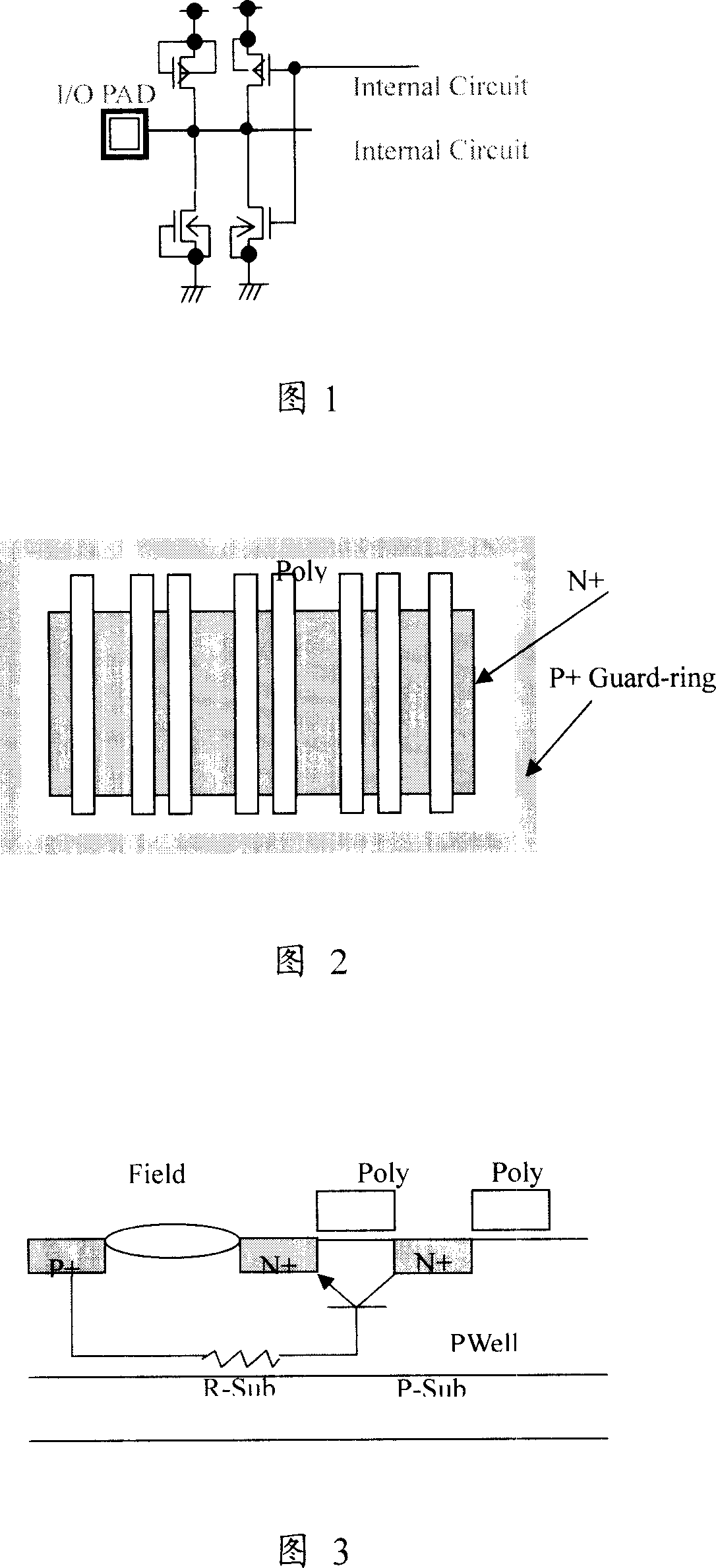
[0016] As shown in FIG. 4 , an ESD protection element structure of the present invention improves the traditional layout method by inserting an N-well ring between the Nch Buffer transistor and the well-controlled guard-ring.

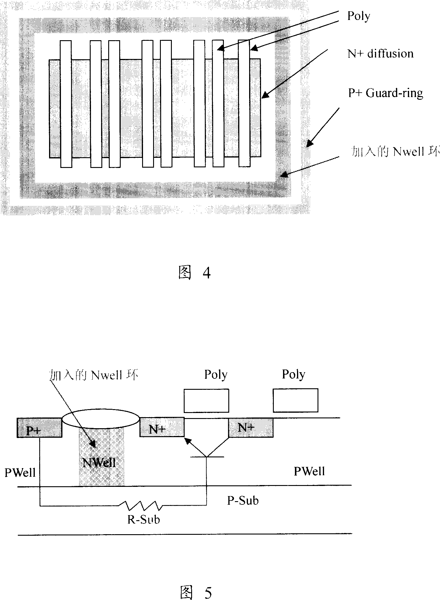
[0017] As shown in Figure 5, from the schematic cross-sectional view of the NMOS, the NMOS element structure is formed on a P-type well of a substrate, and the NMOS element structure includes a gate, which is arranged in the P-type well; a first An N+ diffusion region is arranged in the P-type well and is used as a drain of the NMOS device structure; a second N+ diffusion region is arranged in the P-type well and is used as a source of the NMOS device structure ; A P+ diffusion region is set in the P-type well as a protection ring, and an N well ring is provided between the P+ protection ring and the N+ diffusion region. In addition, the NMOS element structure also includes a plurality of lightly doped drains arranged in the P-type well around the gate,...


PUM


Abstract

This invention relates to a static discharge protection element structure, in which, a N trap ring is plugged between a Nch Buffer transistor and a guard-ring controlled by the trap to increase the volume resistance of all the transistors, when EDS happens, it is easy for them to enter into an breakdown and conduction state, and all finger transistors can act uniformly and enter into a protection state so as to get a strong protection result quickly.

Description

technical field [0001] The invention relates to an electrostatic discharge protection element structure, in particular to an electrostatic discharge protection element structure which improves trigger efficiency. Background technique [0002] Electrostatic discharge (ESD) is an instantaneous energy release process in which a large amount of external energy passes through an integrated circuit, and the entire amplification process is about 100 nanoseconds. In such a short period of time, hundreds of volts, or even thousands of volts of ESD stress have to be released. If the release process is not appropriate, it is easy to cause damage to the components in the integrated circuit. [0003] With the development of semiconductor integrated circuit technology, the requirements for chip integration are getting higher and higher. In deep sub-micron complementary metal-oxide-semiconductor (CMOS) technology, shallower junction depth, thinner gate oxide thickness, adding lightly dop...

Claims


Application Information

Patent Timeline
Patent Type & Authority Applications(China)
IPC IPC(8): H01L27/02H01L23/60
Inventor 徐向明
Owner SHANGHAI HUA HONG NEC ELECTRONICS
Why Eureka
Try Eureka