Printed circuit board and method of manufacturing the same

A printed circuit board, circuit board technology, applied in the directions of printed circuit manufacturing, printed circuits, printed circuits, etc., can solve the problems of restricting the formation of precision circuits, unfavorable environmental protection, and surface roughness expansion.

Inactive Publication Date: 2007-06-27
SAMSUNG ELECTRO MECHANICS CO LTD
View PDF0 Cites 12 Cited by
  • Summary
  • Abstract
  • Description
  • Claims
  • Application Information

AI Technical Summary

Problems solved by technology

However, in conventional SAP, since the copper layer is formed by wet processing such as wet surface treatment and electroless plating, the surface roughness is

Method used


Image

  • Printed circuit board and method of manufacturing the same
  • Printed circuit board and method of manufacturing the same
  • Printed circuit board and method of manufacturing the same

Examples


example 1

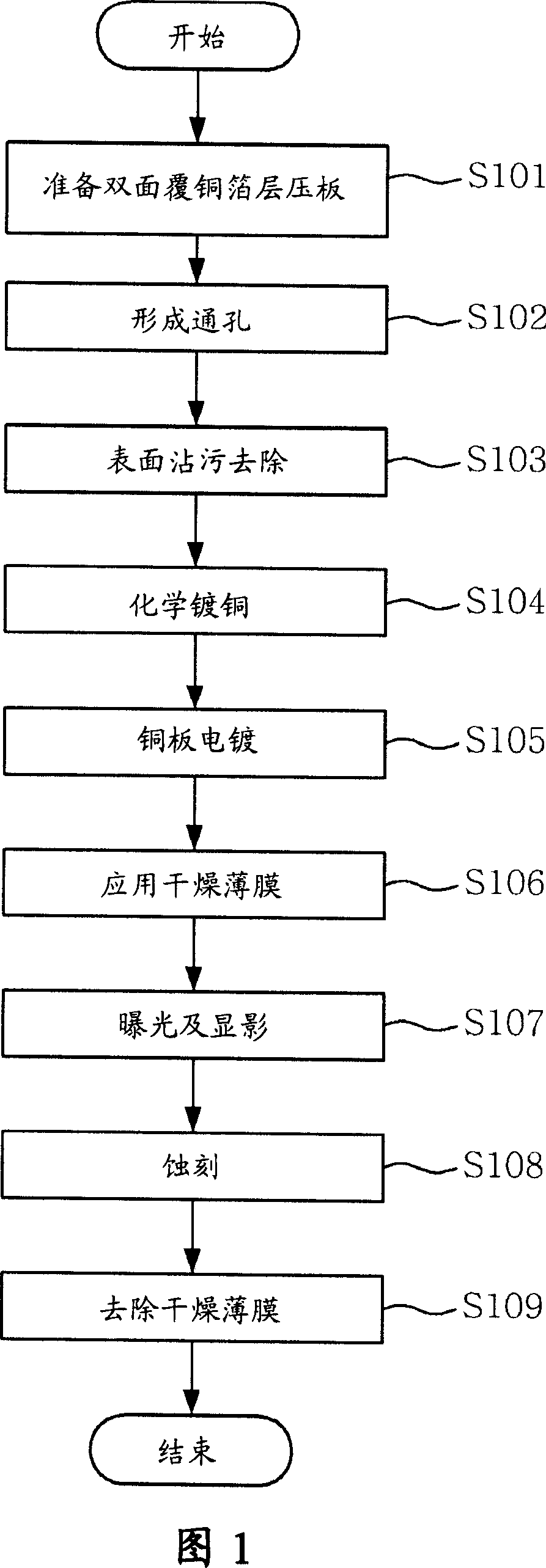
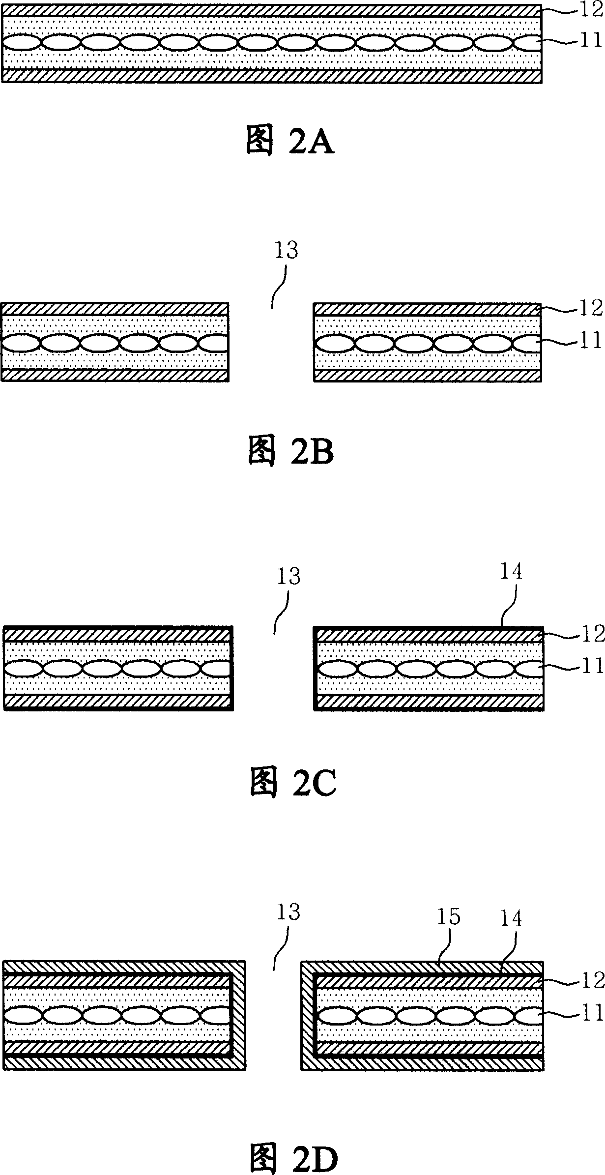
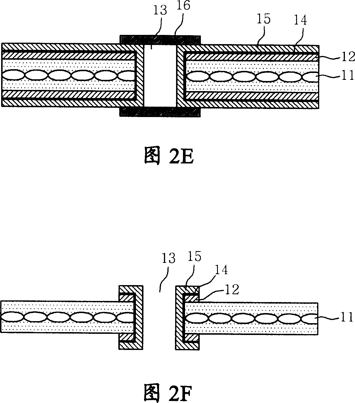
[0083] The two surfaces of the polymer resin substrate used as the base material are repeatedly coated with PTFE under the conditions of temperature 350-420°C and humidity

[0084] The peel strength and surface roughness of the PCBs thus produced were measured. The results are shown in Table 2 below.

example 2

[0086] The two surfaces of the polymer resin substrate used as the base material are repeatedly coated with TPI under the conditions of temperature 250-350 ° C and humidity < RH 50%, so as to form a fluoride ion resin coating with a thickness of about 3 μm. Then, a through hole about 40 μm deep was formed in the substrate, and then an ion beam surface treatment was applied to the substrate using N2 gas under the conditions of an accelerating voltage of about 10 KeV and an ion amount of 2E17. Subsequently, on the surface-treated substrate, a copper layer was deposited to a thickness of about 2 μm using DC sputtering and ion beam sputtering. Finally, a pattern plating process was performed so that the 40 μm deep via hole was filled and a copper pattern plating layer having a thickness of 15 μm was formed.

[0087] The peel strength and surface roughness of the PCBs thus produced were measured. The results are shown in Table 2 below.


PUM

PropertyMeasurementUnit
Thicknessaaaaaaaaaa
Thicknessaaaaaaaaaa
Thicknessaaaaaaaaaa

Abstract

Disclosed are a printed circuit board and a method of manufacturing the same, in which a fluorine resin coating layer is formed on a resin substrate, and then a copper layer is formed using a dry process including ion beam surface treatment and vacuum deposition instead of a conventional wet process including surface roughening and electroless copper plating. According to this invention, the interfacial adhesion of the substrate material may be increased without changing the surface roughness thereof, thus realizing a highly reliable fine circuit. As well, a low dielectric constant and a low loss coefficient may be obtained thanks to the formation of the fluorine resin layer. Further, a wet process is replaced with a dry process, whereby the copper plating layer may be formed in an environmentally friendly manner.

Description

[0001] Related Application Cross Reference [0002] This application claims Korean Patent Application No. 2005-125249, filed on December 19, 2005, entitled "Printed Circuit Board and Method for Manufacturing It" and filed on July 6, 2006, entitled "Printed Circuit Board and Its Priority of Korean Patent Application No. 2006-63370 for Preparation Method", the entire contents of which are incorporated herein by reference. technical field [0003] The present invention relates to a printed circuit board (PCB) and a method of manufacturing the same. Specifically, the present invention relates to a PCB and a method of manufacturing the same, wherein a hydrophilic fluororesin coating is formed on a resin substrate, and a dry plating process replaces a conventional wet plating process, whereby And get high durability precision circuit. Background technique [0004] Currently, PCBs are manufactured using subtractive process, MSAP (modified semi-additive process) or SAP (semi-addit...

Claims


Application Information

Patent Timeline
IPC IPC(8): H05K3/38H05K3/18H05K1/00
CPCH05K3/18H05K3/381H05K2201/0154
Inventor 宋宗锡金泰勋
Owner SAMSUNG ELECTRO MECHANICS CO LTD
Why Eureka
Try Eureka