
Control method of polishing technology

A control method and process control technology, which is applied in the control of workpiece feed motion, grinding/polishing equipment, manufacturing tools, etc., can solve the problem of copper residue on the crystal edge, affecting yield and reliability, and the electrical properties of double metal damascene structures. Uneven problems, to achieve uniform electrical properties, to avoid the effect of crystal edge copper residue

Active Publication Date: 2007-07-04
UNITED MICROELECTRONICS CORP
View PDF0 Cites 5 Cited by
  • Summary
  • Abstract
  • Description
  • Claims
  • Application Information

AI Technical Summary

Problems solved by technology

However, the result of chemical mechanical polishing will be affected by many non-process parameters, which will affect the yield and reliability (Reliability)
[0004] For example, in the dual damascene process, the thickness of the electroplated copper film is usually thicker at the periphery of the wafer, so after chemical mechanical polishing, copper residues on the crystal edge are often caused, or the central area is over-polished (Over Polish) Problems such as dishing and dishing lead to electrical unevenness of the dual damascene structure in each area of ​​the wafer

Method used


Image

  • Control method of polishing technology
  • Control method of polishing technology
  • Control method of polishing technology

Examples


Embodiment Construction

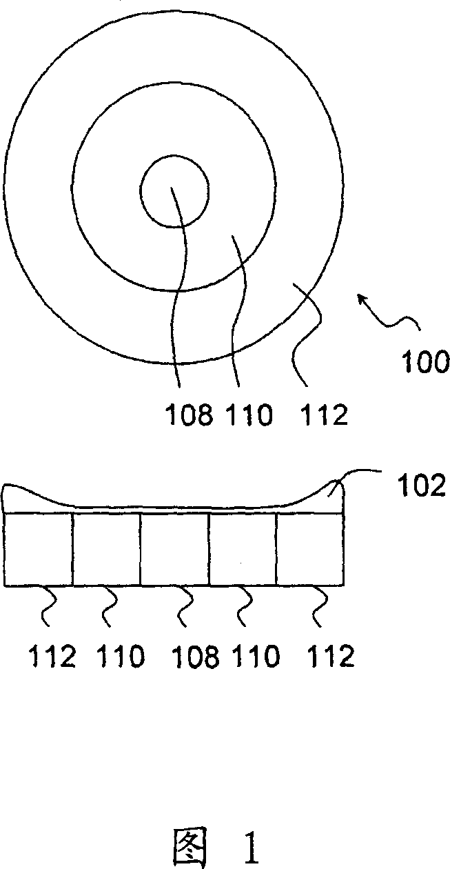
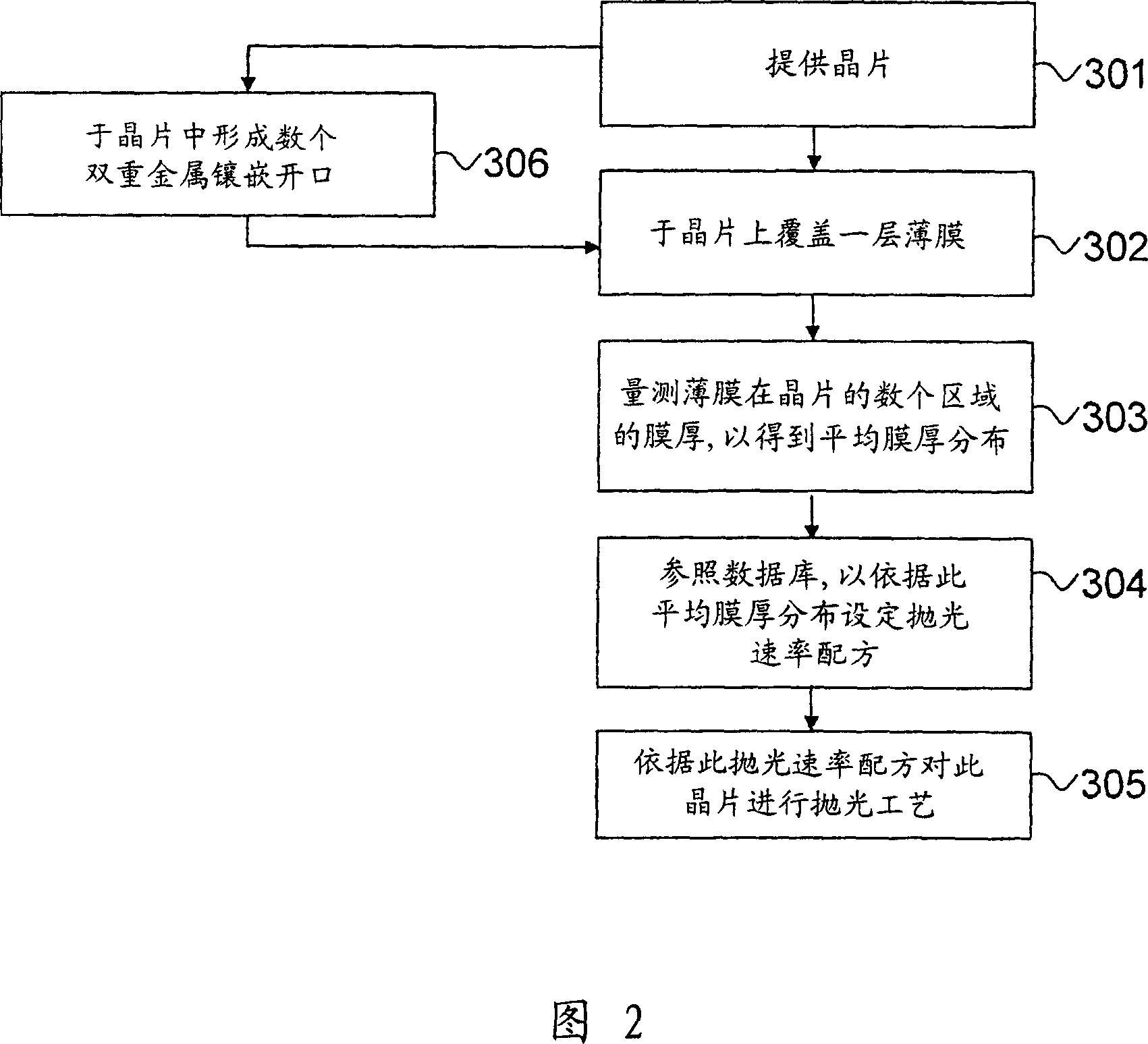
[0041] FIG. 1 is a top view of a wafer 100 and a schematic cross-sectional view along the section line II' according to an embodiment of the present invention. FIG. 2 is a flowchart of a control method for a polishing process according to an embodiment of the invention.

[0042] Please refer to FIG. 1 and FIG. 2 at the same time. Firstly, step 301 is performed: providing the wafer 100 . The wafer 100 is, for example, a 12-inch wafer. Then proceed to step 302 : covering the wafer 100 with a thin film 102 . The material of the thin film 102 is copper, for example. The method of forming the thin film 102 is, for example, an electroplating method or a chemical vapor deposition method.

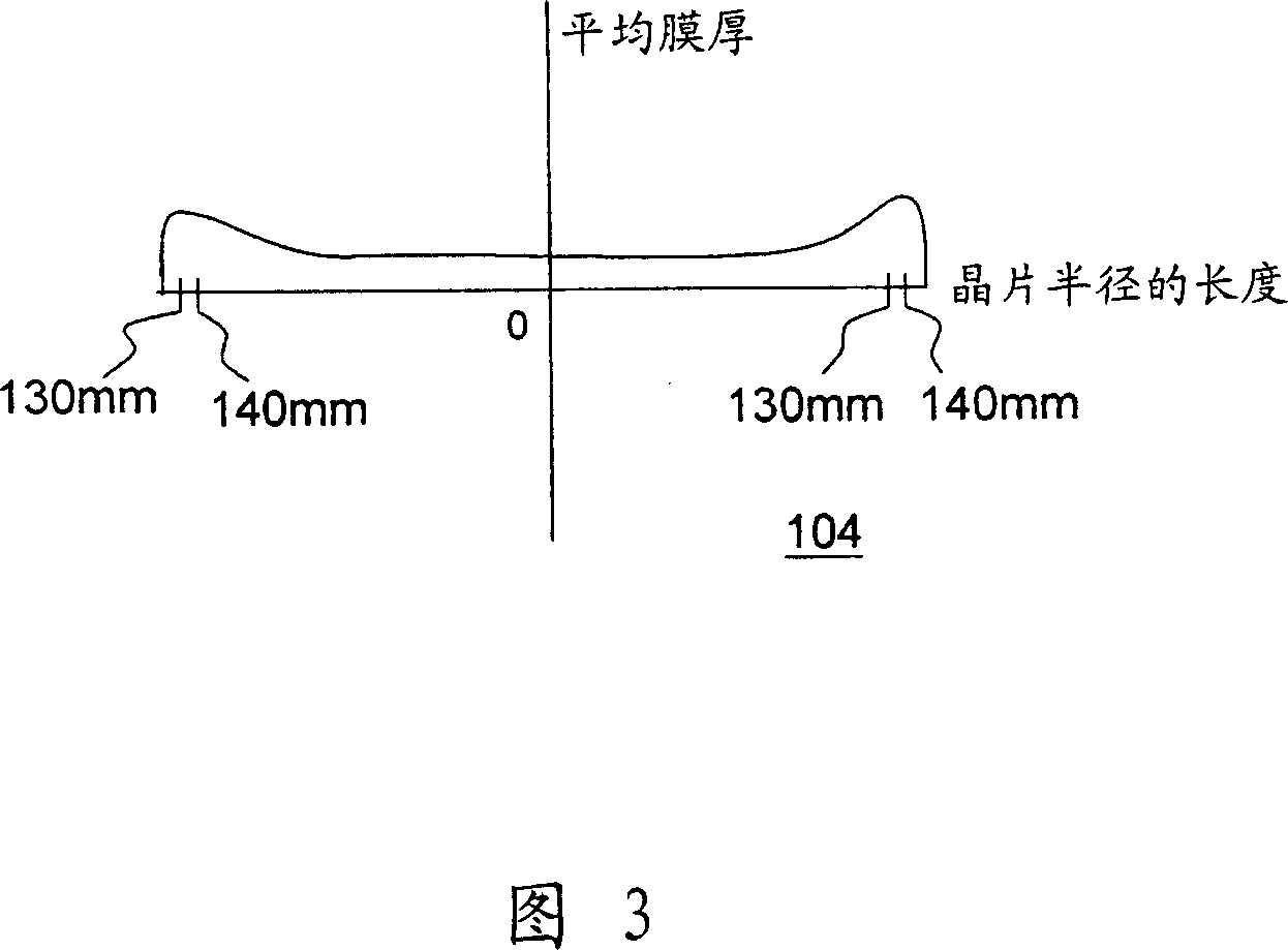
[0043] Next, proceed to step 303 : measure the film thicknesses of the thin film 102 in several regions of the wafer 100 to obtain the average film thickness distribution 104 shown in FIG. 3 . "Distribution of average film thickness" is, for example, a function of wafer radius length and averag...


PUM


Abstract

It is a polishing process control method. First, provide a chip, and the chip has been covered with a thin film layer. Measuring thin film thickness on the chip's several regions, in order to obtain the average film thickness distribution. Thereafter, according to the average film thickness distribution, it sets a polishing rate formula. Then, based on this polishing rate formula, it processes the polishing technique to the chip. This method can improve the film thickness uniformity after polishing, and furthermore improve the efficiency of polishing technique and yield of the chip.

Description

technical field [0001] The invention relates to a control method of a semiconductor process, in particular to a control method of a polishing process. Background technique [0002] Chemical mechanical polishing technology has been widely used in the fabrication of structures such as double damascene, metal plugs, upper electrodes of trench capacitors (Trench Capacitor) and the planarization of dielectric layers. It is an indispensable process for the manufacture of integrated circuits. [0003] The main process parameters in the chemical mechanical polishing process include the pressure applied by the polishing head, the composition of the polishing liquid and the polishing grains, the material of the polishing pad, the relative linear velocity and temperature of the wafer and the polishing pad, etc. However, the result of chemical mechanical polishing will be affected by many non-process parameters, which will affect the yield and reliability (Reliability). [0004] For ex...

Claims


Application Information

Patent Timeline
Patent Type & Authority Applications(China)
IPC IPC(8): H01L21/321H01L21/304H01L21/768H01L21/66B24B49/02
Inventor 邓清文林进坤梁文中
Owner UNITED MICROELECTRONICS CORP
Learn More