

TFT array semi-exposure photoetching technology
A lithography process and semi-exposure technology, which is applied in photosensitive material processing, micro-lithography exposure equipment, and photolithography exposure equipment, etc., can solve the problems of high production cost and large number of processes, so as to increase production capacity and shorten the production time. The effect of process time and cost saving
- Summary
- Abstract
- Description
- Claims
- Application Information
AI Technical Summary
Problems solved by technology
Method used
Image

Examples
Embodiment Construction
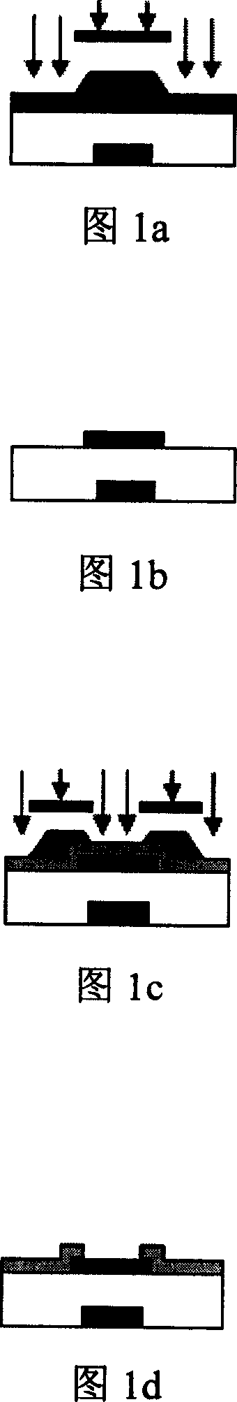
[0011] The preferred embodiments of the present invention are given below in conjunction with the accompanying drawings to describe the technical solution of the present invention in detail.
[0012] As shown in Figures 1a-1d, a TFT array semi-exposure photolithography process, a photomask plate with a pattern lower than the critical resolution of the exposure equipment is set at the channel position of the thin film transistor, and a semiconductor film layer and a metal film have been formed. A photolithographic process is carried out on the substrate of the layer.
[0013] After the first wet etching of the metal film layer and the dry etching of the semiconductor, the photoresist remaining in the previous step is etched to remove the residual photoresist in the channel part, and then the metal film layer is subjected to the second step. Second wet etching.
[0014] For a glass substrate that already has a gate pattern and has formed a semiconductor film layer and a metal f...
PUM
 Abstract
Description
Claims
Application Information