Imaging device, monitoring device, and electronic device

a monitoring device and imaging device technology, applied in the direction of transistors, color televisions, television systems, etc., can solve the problems of large power consumption of analog/digital, achieve novel structure, reduce power consumption of entire imaging devices, and reduce power consumption. effect of digital processing

Active Publication Date: 2018-07-10
SEMICON ENERGY LAB CO LTD
View PDF147 Cites 5 Cited by
  • Summary
  • Abstract
  • Description
  • Claims
  • Application Information

AI Technical Summary

Benefits of technology

[0009]To further reduce power consumption of the entire imaging device, it is important to reduce power required for digital processing and power required for analog processing for controlling digital processing.
[0010]An object of one embodiment of the present invention is to provide a novel imaging device, a novel display device, a novel electronic device, or the like. Another object of one embodiment of the present invention is to provide an imaging device or the like with a novel structure and low power consumption.
[0017]One embodiment of the present invention can provide a novel imaging device, a novel display device, a novel electronic device, or the like. Another embodiment of the present invention can provide an imaging device or the like with a novel structure and low power consumption.

Problems solved by technology

Accordingly, to generate the determination signal, a vast amount of power is consumed by A / D (analog / digital) conversion of the data read out from the CMOS image sensor, data transfer for taking a large amount of digital data into the computer, storage and reading of the digital data in / from a memory device in the computer, execution of the image processing software, and the like.

Method used


Image

  • Imaging device, monitoring device, and electronic device
  • Imaging device, monitoring device, and electronic device
  • Imaging device, monitoring device, and electronic device

Examples


embodiment 1

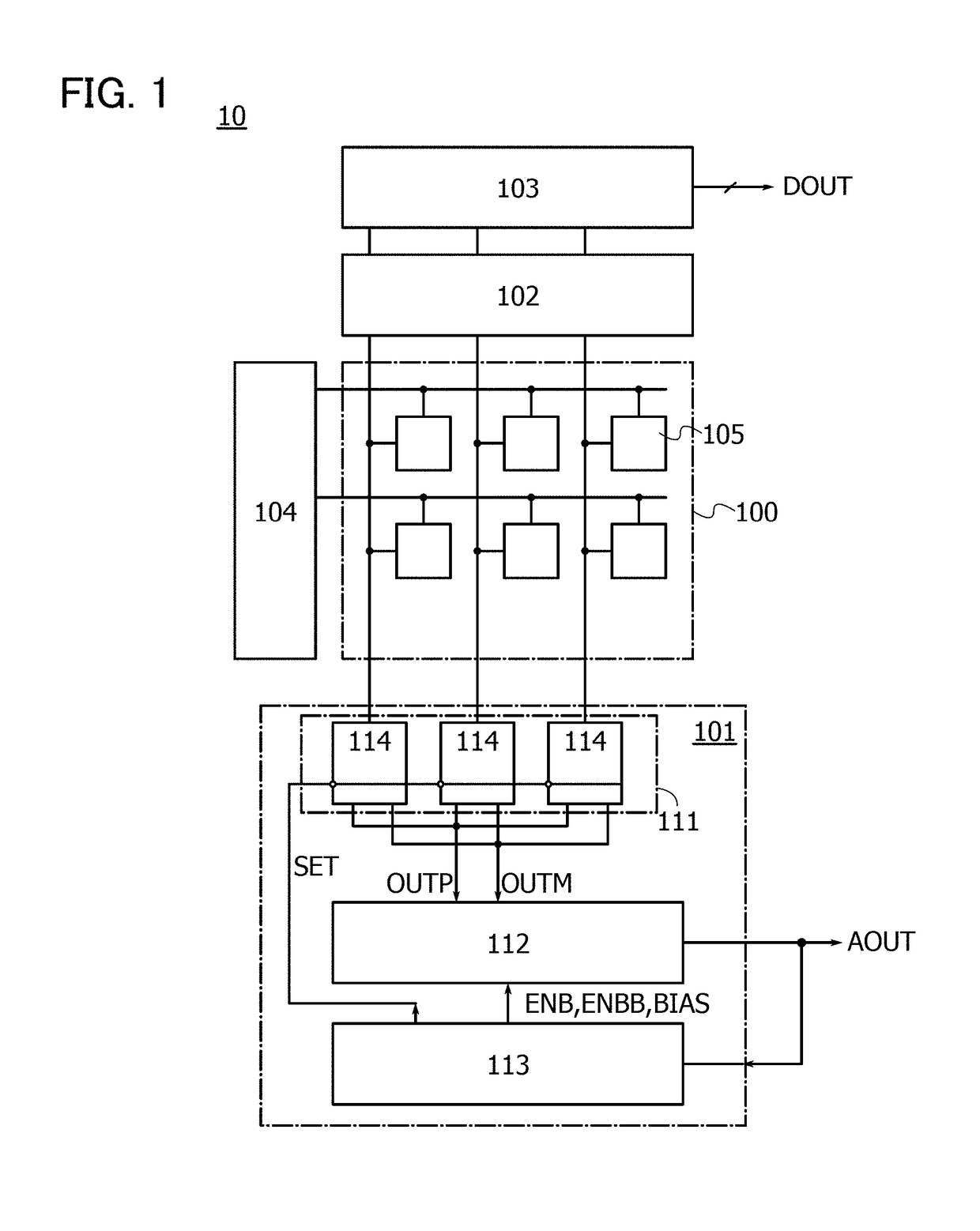
[0067]The configuration of an imaging device in one embodiment of the present invention will be described with reference to FIG. 1.

[0068]In this specification and the like, an imaging device refers to any device having an image capturing function, or alternatively refers to a circuit having an image capturing function or a whole system including the circuit.

[0069]FIG. 1 is a block diagram illustrating the configuration of the imaging device in one embodiment of the present invention.

[0070]In FIG. 1, an imaging device 10 includes a pixel portion 100, an analog processing circuit 101, an A / D converter circuit 102, a column driver 103, and a row driver 104. The pixel portion 100 includes pixels 105. The analog processing circuit 101 includes a constant current circuit 111, a current comparison circuit 112, and a control circuit 113. The constant current circuit 111 includes constant current sources 114 corresponding to columns of the pixels 105.

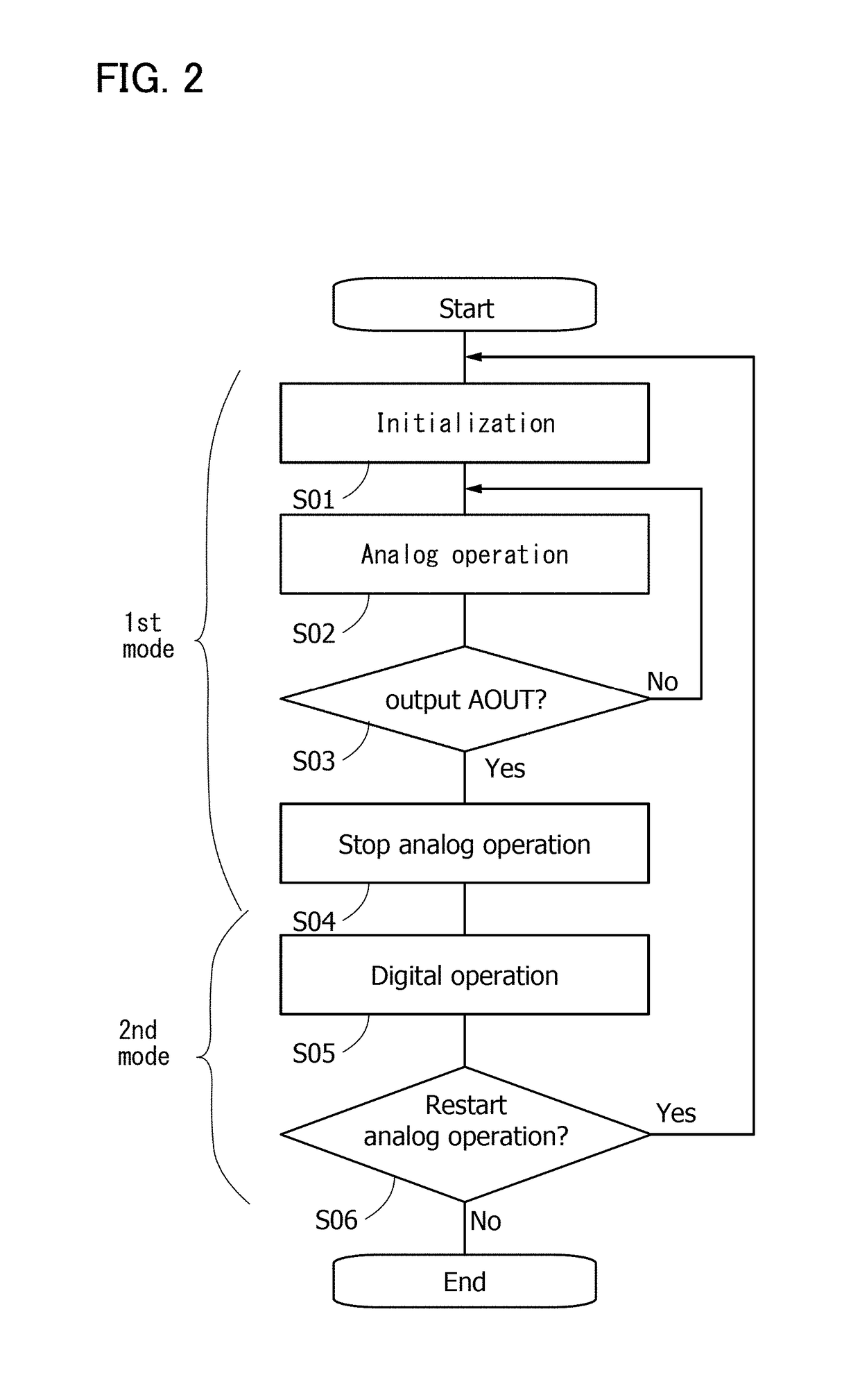
[0071]The imaging device 10 operates in a...

embodiment 2

[0091]This embodiment will explain specific configuration examples of the constant current circuit, the current comparison circuit, and the control circuit included in the analog processing circuit described in Embodiment 1. In this embodiment, the description of the components is based on a configuration that is actually designed; thus, specific numerals used for describing the operation, such as the number of pixels and wirings provided in the row direction and column direction and the frequency of a clock signal and the like, are merely examples.

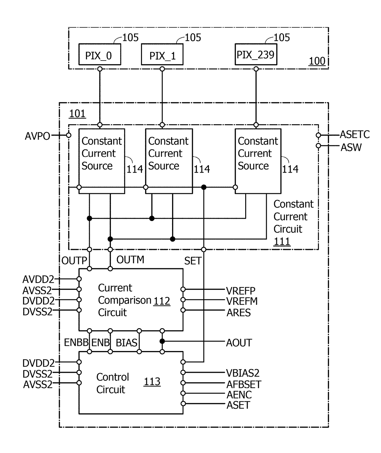
[0092]FIG. 3 is a block diagram illustrating the analog processing circuit 101 and the pixels 105 in the pixel portion 100 electrically connected to the analog processing circuit 101. FIG. 3 illustrates an example where pixels 105 of 240 columns (only first, second, and 240th columns are shown) are provided.

[0093]In the constant current circuit 111, the constant current source 114 is provided for each column. The second current flows betw...

embodiment 3

[0134]In this embodiment, a configuration example of the analog processing circuit that is different from that in Embodiment 2 will be described. Note that the description of the portions described in Embodiment 2 is omitted.

[0135]Like FIG. 3, FIG. 11 is a block diagram illustrating the analog processing circuit 101 and the pixels 105 in the pixel portion 100 electrically connected to the analog processing circuit 101. FIG. 12 illustrates the constant current circuit 111 including a constant current source 310 having a configuration different from that in FIG. 4.

[0136]The configuration of FIG. 11 differs from that of FIG. 3 in that a potential AVREF is supplied instead of the signal ASETC. The configuration of FIG. 12 differs from that of FIG. 4 in that a transistor 313 whose gate is supplied with the potential AVREF is provided instead of the transistors 303 and 304 and the capacitor 307.

[0137]In the constant current circuit 111 of FIG. 11, the potential AVREF is supplied instead o...


PUM


Abstract

An imaging device includes a pixel; a digital circuit; and an analog processing circuit including a constant current circuit, a current comparison circuit, and a control circuit. The pixel is capable of outputting differential data. The constant current circuit is capable of supplying a first current corresponding to the differential data, in accordance with a first control signal. The current comparison circuit is capable of supplying a second current that flows through the constant current circuit in accordance with a change in the differential data. The current comparison circuit has a function of setting a determination signal active depending on whether to supply the second current to the constant current circuit. The control circuit has a function of controlling the constant current circuit and the current comparison circuit to stop their functions as the determination signal becomes active. The digital circuit operates as the determination signal becomes active.

Description

BACKGROUND OF THE INVENTION[0001]1. Field of the Invention[0002]One embodiment of the present invention relates to an imaging device, a monitoring device, and an electronic device.[0003]Note that one embodiment of the present invention is not limited to the above technical field. The technical field of the invention disclosed in this specification and the like relates to an object, a method, or a manufacturing method. In addition, one embodiment of the present invention relates to a process, a machine, manufacture, or a composition of matter. Specific examples of the technical field of one embodiment of the present invention disclosed in this specification include a semiconductor device, a display device, a light-emitting device, a power storage device, an imaging device, a memory device, a method for driving any of them, and a method for manufacturing any of them.[0004]2. Description of the Related Art[0005]Imaging devices are generally incorporated in mobile phones and have come i...

Claims


Application Information

Patent Timeline
Patent Type & Authority Patents(United States)
IPC IPC(8): H04N5/378H04N5/32H04N5/232H04N5/369H04N5/33
CPCH04N5/3698H04N5/23241H04N5/378H04N5/332H04N5/369H04N5/32H04N23/11H04N25/709H04N25/70H04N25/75H01L27/14643H01L27/14612H01L27/14636H01L27/14627H01L27/1462H04N25/00H04N25/77
Inventor OHMARU, TAKURO
Owner SEMICON ENERGY LAB CO LTD
Why Eureka
Try Eureka