Photonic-crystal all-optical and-transformation logic gate

a technology of photonic crystal and logic gate, applied in logic circuits, pulse techniques, instruments using specific components, etc., can solve the problems of difficult manufacturing of quantum optical-logic devices and nanomaterial optical-logic devices, and achieve the effects of strong anti-interference capability, compact structure and easy integration with other devices

Inactive Publication Date: 2018-08-07
OUYANG ZHENGBIAO
View PDF2 Cites 2 Cited by
  • Summary
  • Abstract
  • Description
  • Claims
  • Application Information

AI Technical Summary

Benefits of technology

[0007]The present invention is aimed at overcoming the defects of the prior art and providing an all-optical AND-transformation logic gate which is compact in structure, strong in anti-interference capability and easy to integrate with other optical-logic elements.
[0017]Compared with the prior art, the present invention has the following advantages:
[0019]2. Strong anti-interference capability, and ease of integration with other optical-logic elements; and
[0020]3. High contrast of high and low logic outputs, and fast operation.

Problems solved by technology

For modern manufacturing processes, however, the quantum optical-logic devices and the nanomaterial optical-logic devices are very difficult to be manufactured, whereas the PhC optical-logic devices have competitive advantages in terms of manufacturing process.

Method used


Image

  • Photonic-crystal all-optical and-transformation logic gate
  • Photonic-crystal all-optical and-transformation logic gate
  • Photonic-crystal all-optical and-transformation logic gate

Examples


Embodiment Construction

[0028]The terms a or an, as used herein, are defined as one or more than one, the term plurality, as used herein, is defined as two or more than two, and the term another, as used herein, is defined as at least a second or more.

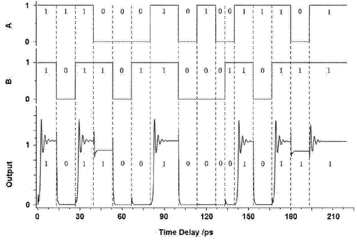
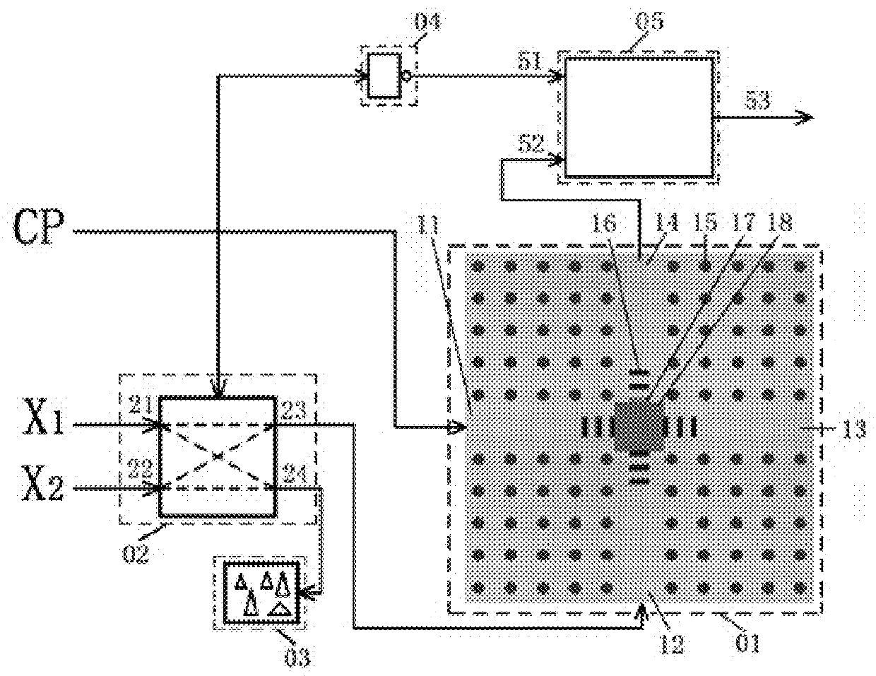
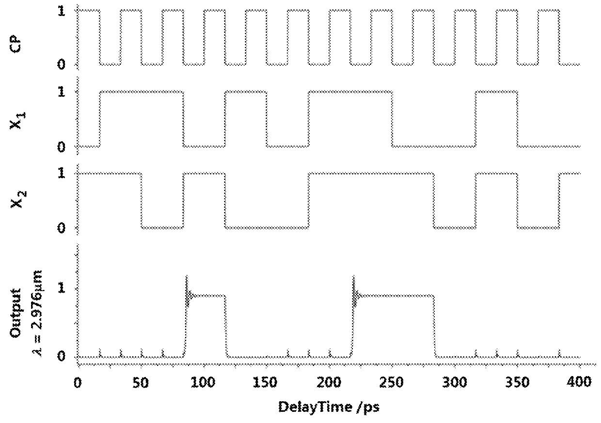
[0029]As shown in FIG. 1, the PhC all-optical AND-transformation logic gate of the present invention includes a PhC-structure unit 01, an optical-switch unit 02, a wave-absorbing load 03, a NOT-logic gate 04 and a D-type flip-flop 05; the PhC-structure unit 01 is a 2D-PhC cross-waveguide nonlinear cavity and is arranged behind the optical-switch unit, the background filling material for the 2D PhC is air or a different low-refractive-index medium with a refractive index less than 1.4, the cross section of the high-refractive-index dielectric pillar of the 2D PhC is circular, oval, triangular or polygonal, the 2D-PhC cross-waveguide nonlinear cavity is a 2D-PhC cross-waveguide four-port network formed by high-refractive-index dielectric pillars, the four-port ...


PUM

PropertyMeasurementUnit
refractive indexaaaaaaaaaa

Abstract

The present invention discloses a photonic crystal (PhC) all-optical AND-transformation logic gate, which comprises a PhC-structure unit, an optical-switch unit, a wave-absorbing load, a NOT-logic gate and a D-type flip-flop; two intermediate-signal output ports of the optical-switch unit are respectively connected with the intermediate-signal input port and the wave-absorbing load of the PhC-structure unit; a clock-signal CP input port is connected with three-branch waveguide, and three output ports are respectively connected with first clock-signal CP input port of the optical-switch unit, second clock-signal CP input port of the PhC-structure unit and the NOT-logic-gate input port; the NOT-logic-gate output port is connected with third clock-signal CP input port of the D-type flip-flop; the signal-output port of the PhC-structure unit is connected with the D-signal input port of the D-type flip-flop. The structure of the present invention is compact in structure and ease of integration with other optical-logic elements.

Description

CROSS-REFERENCE TO RELATED APPLICATION[0001]This application is a continuation application of PCT Application No. PCT / CN2015 / 097848 filed on Dec. 18, 2015, which claims priority to Chinese Patent Application No. 201410799714.3 filed on Dec. 19, 2014, the entire contents of which are hereby incorporated by reference.FIELD OF THE INVENTION[0002]The present invention relates generally to two-dimensional (2D) photonic crystal (PhC) optical AND-transformation logic gates.BACKGROUND OF THE INVENTION[0003]In 1987, the concept of PhC was proposed separately by E. Yablonovitch from United States Bell Labs who discussed how to suppress spontaneous radiation and by S. John from Princeton University who made discussions about photonic localization. The PhC is a material structure in which dielectric materials are arranged periodically in space, and is usually an artificial crystal consisting of two or more materials having different dielectric constants.[0004]With the emergence of and in-depth ...

Claims


Application Information

Patent Timeline
Patent Type & Authority Patents(United States)
IPC IPC(8): G02F3/00G02B6/122G02B6/125G02F1/365G02B6/12B82Y20/00
CPCG02B6/1225G02B6/125G02F1/365G02F3/00B82Y20/00G02B2006/1213G02F2202/32
Inventor OUYANG, ZHENGBIAOYU, QUANQIANG
Owner OUYANG ZHENGBIAO
Why Eureka
Try Eureka