Data bit inversion tracking in cache memory to reduce data bits written for write operations

Active Publication Date: 2018-10-30
QUALCOMM INC
View PDF25 Cites 10 Cited by
  • Summary
  • Abstract
  • Description
  • Claims
  • Application Information

AI Technical Summary

Benefits of technology

[0007]Aspects disclosed in the detailed description include data bit inversion tracking in cache memory to reduce data bits written for write operations. Reducing the number of data bits written to memory can reduce power consumption as an example. In this regard, in exemplary aspects disclosed herein, a memory system is provided that includes a main memory or system memory for storing data. The memory system also includes a cache memory for storing cached versions of the data stored in the main memory. The cache memory includes a cache controller and a cache array. The cache array includes one or more cache entries, each of which includes a cache data field for storing cached data from the main memory and a corresponding bit change track field. In a write operation, in response to a cache hit in the cache memory, the cache controller is configured to compare a current cache data word stored in a cache entry corresponding to a memory address of the write operation to a new data word in

Problems solved by technology

However, compared to SRAM, MRAM write operations typically require more power because a sufficient current must be generated to cause the free layer in an MRAM bit cell to set its magnetic orientation.
While the MRAM controller 106 in the MRAM macro 102 in FIG. 1 can imple

Method used


Image

  • Data bit inversion tracking in cache memory to reduce data bits written for write operations
  • Data bit inversion tracking in cache memory to reduce data bits written for write operations
  • Data bit inversion tracking in cache memory to reduce data bits written for write operations

Examples


Embodiment Construction

[0022]With reference now to the drawing figures, several exemplary aspects of the present disclosure are described. The word “exemplary” is used herein to mean “serving as an example, instance, or illustration.” Any aspect described herein as “exemplary” is not necessarily to be construed as preferred or advantageous over other aspects.

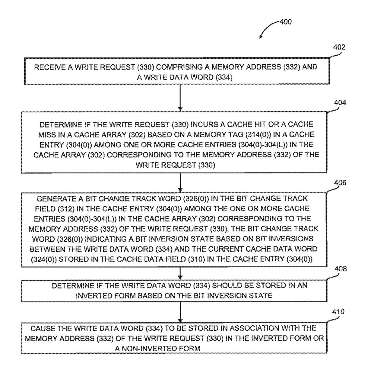
[0023]Aspects disclosed in the detailed description include data bit inversion tracking in cache memory to reduce data bits written for write operations. Reducing the number of data bits written to memory can reduce power consumption as an example. In this regard, in exemplary aspects disclosed herein, a memory system is provided that includes a main memory or system memory for storing data. The memory system also includes a cache memory for storing cached versions of the data stored in the main memory. The cache memory includes a cache controller and a cache array. The cache array includes a plurality of cache entries, each of which include a cache d...


PUM


Abstract

Data bit inversion tracking in cache memory to reduce data bits written for write operations is disclosed. In one aspect, a cache memory including a cache controller and a cache array is provided. The cache array includes one or more cache entries, each of which includes a cache data field and a bit change track field. The cache controller compares a current cache data word to a new data word to be written and stores a bit track change word representing the difference (i.e., inverted bits) between the current cache data word and the new data word in the bit change track field. By using the bit track change word stored in the bit change track field to determine whether fewer bit writes are required to write data in an inverted or a non-inverted form, power consumption can be reduced for write operations through reduced bit write operations.

Description

BACKGROUNDI. Field of the Disclosure[0001]The technology of the disclosure relates generally to memory systems provided in processor-based systems for storing data, and more particularly to memory systems that include the capability of storing data in an inverted form in memory to reduce data bit write operations.II. Background[0002]Semiconductor storage devices are incorporated in integrated circuits (ICs) in electronic devices to provide data storage. One example of a semiconductor storage device is static random access memory (SRAM). Another example of a semiconductor storage device is magneto-resistive random access memory (MRAM). It may be advantageous to use MRAM in place of SRAM for memory applications because MRAM is non-volatile memory in which data is stored by programming a magnetic tunnel junction (MTJ) as part of an MRAM bit cell. An advantage of MRAM is that MTJs in MRAM bit cells can retain stored information even when power is turned off. This is because data is stor...

Claims


Application Information

Patent Timeline
IPC IPC(8): G11C11/16G06F11/10G06F13/42H03M13/29G11C29/04G11C13/00G11C29/50
CPCG11C13/0069G11C11/1673G06F13/4204G06F11/1012G06F11/1048H03M13/2906G11C11/1655G11C29/50G11C2029/0411G11C2013/0076G11C7/1006G11C11/4063G11C11/1675G11C15/00G11C15/02G11C15/046G06F12/0895G06F2212/6046Y02D10/00
Inventor SHIN, HYUNSUKKIM, JUNG PILLKIM, SUNGRYUL
Owner QUALCOMM INC
Why Eureka
Try Eureka