Charged particle beam device and charged particle beam measurement method

a technology of charged particle beam and beam device, which is applied in the direction of basic electric elements, electric discharge tubes, electrical equipment, etc., can solve problems such as image disturbance such as drift or shading

Active Publication Date: 2018-11-06
HITACHI HIGH-TECH CORP
View PDF13 Cites 2 Cited by
  • Summary
  • Abstract
  • Description
  • Claims
  • Application Information

AI Technical Summary

Benefits of technology

[0013]According to the invention of the application, high-accuracy detection can be realized while securing the stability of detected signals in a charged particle beam device or a charged particle beam measurement method.

Problems solved by technology

In particular, when a target to be analyzed is an insulator, the sample is charged by the irradiation of the electron beam, resulting in image disturbance such as drift or shading.

Method used


Image

  • Charged particle beam device and charged particle beam measurement method
  • Charged particle beam device and charged particle beam measurement method
  • Charged particle beam device and charged particle beam measurement method

Examples


first embodiment

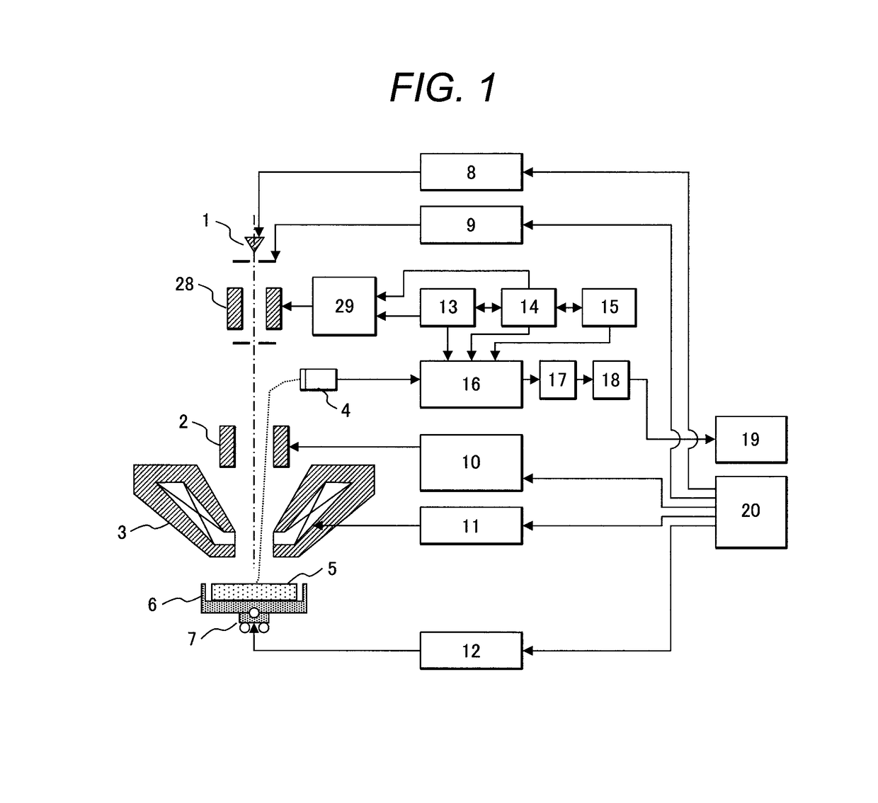
[0033]In the embodiment, a measurement device and method for the amount of secondary electron emissions in which a time reference is provided will be described using an example of a scanning electron microscope among charged particle beam devices. A configuration example of a scanning electron microscope according to the embodiment is shown in FIG. 1. The scanning electron microscope has an electron optical system, a stage mechanism system, an SEM control system, a trigger signal control system, a signal processing system, an SEM operation system, and an electron irradiation control system.

[0034]The electron optical system includes an electron gun 1, a deflector 2, an objective lens 3, and a detector 4. The stage mechanism system includes a sample holder 6 in which a sample 5 is put, and a stage 7 whose inclination can be controlled and which can be moved in the X, Y, and Z axis directions. The SEM control system includes an acceleration voltage control unit 8 for the electron gun, ...

second embodiment

[0054]In the embodiment, an image forming device and method in which the irradiation of a charged particle beam and the detection of secondary electrons are controlled while setting a time reference will be described. A configuration example of a scanning electron microscope in the embodiment is shown in FIG. 8. In addition to the configuration of FIG. 1, the scanning electron microscope of FIG. 8 further includes an image control system and an operation system. The image control system includes an image forming unit 30, and the operation system includes an image display unit 31 and an operation interface 20.

[0055]As similar to Step S100, Step S101, and Step S102 of FIG. 6, the acceleration voltage Va, the current Ip of primary electrons, and the applied voltage Vr to the sample holder are set as the settings of the observation conditions. In the embodiment, Va, Ip, and Vr were 5000 V, 10 pA, and −4700 V, respectively. Further, as similar to Step S103, Step S104, and Step S105 of FI...

third embodiment

[0059]In the embodiment, a measurement device and method of surface potential using the amount of secondary electron emissions will be described. The embodiment will be described using a scanning electron microscope as an example among charged particle beam devices. The same configuration as FIG. 1 was used for the scanning electron microscope in the embodiment.

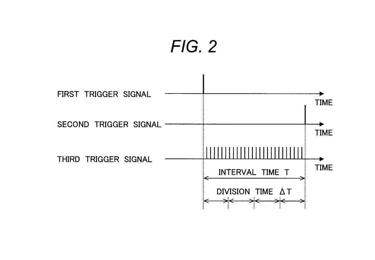
[0060]FIG. 13 shows a GUI 38 for a surface measurement. The GUI 38 includes an operation interface 20 and a measurement result display unit 19. The GUI 38 has an acceleration voltage setting unit 22, a current setting unit 23 of primary electrons, an applied voltage setting unit 24 to a sample holder, an interval time setting unit 25 that inputs an interval time T between a first trigger signal and a second trigger signal, a generation number setting unit 26 for the number of generated third trigger signals N, a division time setting unit 27 that equally divides the interval time, a measurement result display unit 39 of the a...


PUM


Abstract

An object of the present invention is to realize both of the accuracy of measuring the amount of secondary electron emissions and the stability of a charged particle beam image in a charged particle beam device. In a charged particle beam device, extraction of detected signals is started by a first trigger signal, the extraction of the detected signals is completed by a second trigger signal, the detected signals are sampled N times using N (N is a natural number) third trigger signals that equally divide an interval time T between the first trigger signal and the second trigger signal, secondary charged particles are measured by integrating and averaging the signals sampled in respective division times ΔT obtained by equally dividing the interval time T, and the division time ΔT is controlled in such a manner that the measured number of secondary charged particles becomes larger than the minimum number of charged particles satisfying ergodicity.

Description

TECHNICAL FIELD[0001]The present invention relates to a charged particle beam device and a charged particle beam measurement method that observe a sample using a charged particle beam.BACKGROUND ART[0002]As a microscope by which a sample can be enlarged and observed, there is a charged particle microscope using a charged particle beam such as electrons or ions. In particular, a scanning electron microscope (hereinafter, abbreviated as SEM) that images by scanning an electron beam on a sample has been used for a sample analysis such as an observation of a fine surface shape or a local composition analysis. The SEM is a microscope that analyzes a sample in such a manner that an electron beam accelerated by a voltage applied to an electron source is irradiated onto the sample, and the focused electron beam (primary electrons) is scanned on the sample by a deflector.[0003]In particular, when a target to be analyzed is an insulator, the sample is charged by the irradiation of the electro...

Claims


Application Information

Patent Timeline
Patent Type & Authority Patents(United States)
IPC IPC(8): H01J37/244H01J37/26H01J37/28
CPCH01J37/28H01J37/265H01J37/244H01J2237/043
Inventor TSUNO, NATSUKIKIMURA, YOSHINOBUKAZUMI, HIDEYUKIKAWANO, HAJIMETOMIZAWA, JUNICHIRO
Owner HITACHI HIGH-TECH CORP
Why Eureka
Try Eureka